
TL;DR · 30-second read
The Short Version
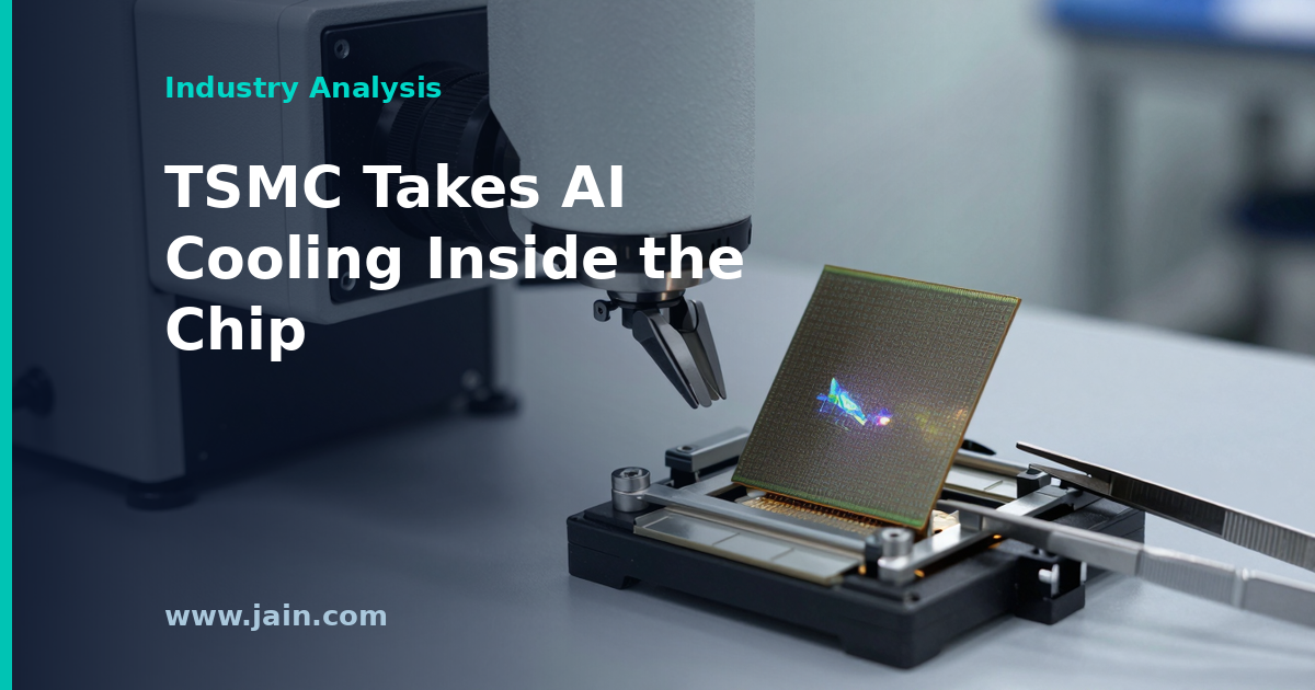
The chips that run artificial intelligence are getting so hot that cooling them from the outside is starting to run out of room. TSMC, the Taiwanese company that manufactures most of the world’s advanced processors, is looking at cutting channels finer than a human hair into the chip itself and pumping liquid through them, right next to where the heat is made.
Forecasts put the power a single artificial intelligence system draws at roughly six times today’s level within five years. If cooling moves inside the chip, the company that builds the chip starts selling the cooling too.
TrendForce reported that TSMC is evaluating microchannel cooling integrated at the chip level — etching or bonding fluid channels directly into the silicon package so coolant flows microns from the transistors — as projected power draw for AI systems rises roughly sixfold over the next five years. The report frames the technology as a response to the point at which conventional external cooling, including metal cold plates strapped to the top of a processor, stops keeping pace with heat generated inside the package.
TSMC has not addressed the technology in its recent filings with United States regulators. Its 6-K filed August 25, 2026 covering July activity reported no board-approved capital appropriations for the month, and its 6-K filed September 1, 2026 dealt with a routine dividend adjustment.
Executive Summary
For a decade, cooling improvements in computing happened outside the chip: better fans, then cold plates, then facility water loops and immersion tanks. Chip-level microchannel cooling breaks that pattern. It puts the coolant inside the package itself, shortening the path heat must travel from transistor to fluid — the single largest source of thermal resistance in a modern accelerator stack. If TSMC productizes it, cooling stops being purely a data center purchase and becomes partly a foundry and advanced-packaging purchase.
The sixfold power projection is the forcing function. Each generation of AI accelerator has raised per-package power while shrinking the area over which that heat can be spread. External cooling can move more fluid faster, but it cannot shorten the distance between the hot spot and the fluid. Microchannels can, which is why the approach has moved from research curiosity toward roadmap discussion.
The commercial implications run in several directions at once: advanced packaging gains value, cold-plate and thermal-interface suppliers face a long-run substitution question, and data center operators inherit a component that is sealed, unserviceable and warranted by the chipmaker rather than the integrator. None of that is settled, and TSMC has published no timeline, node, capacity or customer detail.
Why the Thermal Bottleneck Has Moved Below the Heatsink
Heat leaving a processor passes through a chain of obstacles: the silicon itself, a thermal interface material, a metal lid, another interface layer, and finally a cold plate or heatsink carrying the heat away. Each junction adds resistance. Data center engineering over the past few years has attacked the last link in that chain — swapping air for water, moving from rear-door heat exchangers to direct-to-chip cold plates, adding coolant distribution units. Those changes worked, but they optimise the part of the path furthest from the problem.
Microchannel cooling attacks the first link. By routing fluid through channels formed in or immediately against the silicon, it removes several interface layers and places coolant adjacent to the hot spots rather than millimetres above them. That matters most for the tightly packed, high-power dies used in AI training accelerators, where heat is not evenly distributed and a small area of the die can limit the performance of the whole package.
The projected sixfold rise in AI system power over five years is what makes this urgent rather than academic. Cooling capacity outside the package can be scaled by spending more — bigger pumps, colder water, more plumbing. Thermal resistance inside the package cannot be spent away. Once it dominates, the only remaining lever is to redesign the package, which is precisely where a foundry with leading advanced-packaging capability has an advantage.
Cooling Becomes a Foundry Product
The business consequence is a shift in where cooling value is captured. Today a hyperscaler — an operator of very large cloud data centers — buys accelerators from a chip designer and cooling from a separate thermal supply chain of cold-plate makers, manifold vendors, pump and coolant distribution unit manufacturers. If the highest-value part of the thermal path is fabricated at the packaging stage, part of that spend migrates upstream into the price of the package.
That is a favourable structural position for TSMC, which already assembles AI accelerators using advanced packaging that stacks logic dies and high-bandwidth memory on a shared substrate. Adding fluid channels to that flow extends an existing chokepoint rather than opening a new competitive front. For established thermal suppliers, the risk is gradual rather than immediate: facility-side cooling, plumbing and heat rejection remain necessary regardless, because heat still has to leave the building. What could shrink is the premium attached to the interface between chip and coolant.
There are real costs on the other side of the ledger. A sealed fluid path inside a package is not field-serviceable. Leaks, corrosion, particulate clogging and mechanical stress become manufacturing yield and warranty problems for the chipmaker rather than maintenance problems for the operator. Testing a package that only performs correctly when fluid is flowing complicates production test. Those are engineering problems with known research literature behind them, but solving them at high volume and acceptable yield is a different exercise from demonstrating them.
What TSMC’s Filings Do and Do Not Show
TSMC’s recent disclosures to United States regulators contain nothing about the technology. The 6-K filed on August 25, 2026, which reports the company’s July activity, listed no capital appropriations approved by the board that month, recorded a NT$0.7 billion equity investment disposition, and reported no share pledges or cancellations. The 6-K filed on September 1, 2026 was narrower still: an adjustment of the first-quarter 2026 cash dividend from NT$7.0 to NT$7.00000137 per common share, payable October 8, 2026, after shares were reclaimed from 2024 restricted stock awards.
This absence is not evidence against the programme. Research and early development work does not normally surface in monthly shareholding and appropriation reports, and companies routinely discuss roadmap directions publicly long before they appear as line items. But it does bound what can currently be said: there is no disclosed capital commitment, no announced capacity, and no financial scale attached to chip-level cooling at TSMC.
For investors, that suggests where to look next rather than what to conclude now. Board-approved capital appropriations in the monthly filings, advanced-packaging capacity announcements, and any customer disclosure from accelerator designers would be the first hard signals that microchannel cooling has moved from evaluation to committed investment.
What It Changes for Data Center Buyers — and What It Doesn’t
Operators planning liquid-cooled halls should not read this as a reason to wait. Chip-level cooling reduces resistance inside the package; it does not eliminate the need for a facility water loop, coolant distribution units, heat rejection equipment or the electrical capacity to feed the racks. If anything, a package designed to shed more heat more efficiently makes the facility-side loop more important, because more watts per rack must ultimately be rejected to air, water or the outside environment.
The more consequential change is contractual. Cooling that ships inside the processor moves specification authority to the chipmaker: coolant chemistry, filtration standards, inlet temperature and flow requirements would become conditions of the chip’s warranty rather than choices made by the integrator. Operators used to negotiating thermal design with a systems vendor may find those parameters arriving pre-set.
None of this is imminent. What the direction of travel does justify is designing new capacity for liquid distribution and water quality management as a baseline rather than an upgrade, since every plausible version of the next five years — cold plates, microchannels or both — ends with liquid at the rack.
Background
TSMC is the world’s largest contract chip manufacturer, producing leading-edge processors for companies that design but do not fabricate their own silicon. Its role in AI hardware extends beyond making transistors: its advanced packaging capacity, which bonds logic dies and high-bandwidth memory onto a shared substrate, has been one of the industry’s tightest bottlenecks through the current build-out. As a foreign private issuer listed in New York, TSMC files monthly 6-K reports with United States regulators covering board capital appropriations, asset transactions, bond issuance and insider shareholdings.
Cooling has escalated in parallel. Air cooling gave way to rear-door heat exchangers, then to direct-to-chip cold plates and facility water loops as accelerator power outgrew what fans could handle. Each step moved the working fluid closer to the processor while leaving the package itself untouched. Chip-level microchannel cooling is the logical next step in that sequence — and the first one that would be manufactured by the chipmaker rather than installed by the data center.
Source: [News] TSMC Eyes Chip-Level Microchannel Cooling as AI System Power Could Rise 6× in Five Years — TrendForce report on TSMC’s evaluation of microchannel cooling integrated at the chip level against projected growth in AI system power.
Primary sources: Taiwan Semiconductor Manufacturing Company, Form 6-K filed September 1, 2026 (adjustment to first-quarter 2026 cash dividend per share); Taiwan Semiconductor Manufacturing Company, Form 6-K filed August 25, 2026 (monthly report covering July 2026 shareholdings, asset transactions and capital appropriations).