
TL;DR · 30-second read
The Short Version
Marvell makes chips that move data using light instead of electricity. The company says it has shipped more than five million of them, built with a manufacturing partner, Tower Semiconductor.
That matters because the computers behind artificial intelligence are now so large they no longer fit in one room. Moving data between them fast enough has become a bottleneck, and light is the fix.
Marvell’s most recent quarter set a company revenue record: $2.739 billion, up 37 percent from a year earlier.
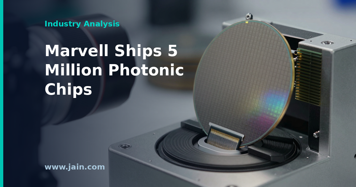
Stocktwits reported on June 18, 2026 that Marvell Technology (NASDAQ: MRVL) said it had shipped more than 5 million coherent photonic integrated circuits to customers worldwide, produced in partnership with specialty foundry Tower Semiconductor, and that Marvell shares rose more than 5% in premarket trading; the same report said the announcement came days before Marvell’s June 22, 2026 entry into the S&P 500, replacing Pool Corporation, and cited Nvidia chief executive Jensen Huang’s earlier description of Marvell as the “next trillion-dollar company.”
The company framed the shipment as a response to component scarcity in the data center market. “This milestone demonstrates the strength of our collaboration,” said Dr. Radha Nagarajan, Marvell’s Senior Vice President and Chief Technology Officer, Optical Engineering, adding that the two companies would “continue working… to advance next-generation coherent technologies for scale across data center architectures.” Two months later, in results reported to the SEC on August 27, Marvell posted record quarterly revenue of $2.739 billion, up 37% year over year, with Data Center revenue growth accelerating to 46%.
Executive Summary
A coherent photonic integrated circuit is a chip that sends and receives information as light rather than as electrical current, encoding data in the phase and amplitude of a laser beam. The technique was developed for long-haul telecom, where signals travel hundreds of kilometres. It has migrated into the data center because AI training and inference clusters have outgrown single buildings, and copper cabling loses too much signal over the distances involved.
The significance of a five-million-unit figure is not technical but industrial. Performance claims are made with a single working part; volume claims require yield, tested wafer capacity, packaging, and a foundry relationship that holds under load. Marvell attaching a unit count to a photonics announcement, rather than a data rate or a power-per-bit number, is a statement that this product line has left the qualification stage.
Marvell’s own financial disclosures give that claim a supportive backdrop without confirming its specifics. In the press release filed as an exhibit to its August 27 Form 8-K, Marvell reported record second-quarter fiscal 2027 revenue of $2.739 billion and guided the current quarter to $3.150 billion, plus or minus 5%. Chairman and CEO Matt Murphy pointed to “strong demand in Connectivity and a significant acceleration in our Custom business.” What the release does not do is size the photonics business itself.
A Unit Count Is a Supply Claim, Not a Speed Claim
Optical interconnect vendors usually announce firsts: the first 800-gigabit module, the first demonstration at a new modulation scheme. Those announcements tell buyers what is possible. A shipment total tells them something different and, for anyone building capacity, more useful — that parts exist in quantity, that they have been through a customer’s qualification process, and that a supplier is willing to be measured against a number it will have to keep growing.
That distinction is the heart of the story. For most of the current AI buildout, optics has been discussed as a constraint: lasers, modulators and the specialty processes that produce them have been among the harder items to source, alongside advanced packaging and memory. A supplier publicly counting units in the millions is signalling that at least one part of that constraint is loosening. It also changes the competitive question from who has the best device to who can produce devices reliably at a price that survives volume, which is the question commodities are settled on.
Buyers should hold the enthusiasm in proportion. The milestone is cumulative and undated — five million units shipped over what period, across how many product generations, and to how many customers are all open. A number that large spread thinly across several years and several generations describes a mature product family; the same number concentrated in recent quarters would describe a genuine volume inflection. Marvell has not said which it is.
The Foundry Half Deserves Equal Billing
Silicon photonics is a specialty manufacturing problem before it is a design problem. Building waveguides, modulators and detectors alongside conventional transistors requires process steps that leading-edge logic foundries generally do not offer, which is why the work concentrates in a small number of specialty fabs. Naming Tower Semiconductor in the announcement is therefore not courtesy — it identifies where the physical capacity actually sits.
This is a real strategic asset and a real dependency at the same time. A designer with a proven, high-yielding photonics platform at a partner fab has a lead that competitors cannot close by hiring engineers alone; process qualification takes years. But the same relationship concentrates risk. If demand for coherent optics keeps compounding at the rate Marvell’s Data Center commentary implies, the binding constraint moves upstream to wafer starts, laser supply and packaging throughput — none of which Marvell controls outright.
Neither company has described the commercial architecture underneath the partnership: whether capacity is contractually reserved, whether the arrangement is exclusive in either direction, or what expansion is planned. Those terms determine how much of a five-million-unit milestone is a durable moat and how much is a snapshot of a good year.
What the August Filings Confirm — and What They Leave Out
Marvell’s fiscal calendar ends in late January, so the quarter reported on August 27 (fiscal Q2 2027) covers the three months to August 1, 2026 — the period immediately following the photonics announcement. The results were strong on their face: revenue of $2.739 billion came in $39.0 million above the midpoint of prior guidance, GAAP net income was $308.0 million ($0.33 per diluted share), non-GAAP net income was $865.9 million ($0.94), and operating cash flow was $605.5 million. The company raised its revenue outlook for both fiscal 2027 and fiscal 2028.
The gap between $0.33 GAAP and $0.94 non-GAAP earnings is worth explaining rather than glossing over. GAAP figures follow standard accounting rules; Marvell’s non-GAAP measures exclude stock-based compensation, amortisation of intangible assets acquired in past deals, restructuring and similar items. The company itself notes in the release that acquired intangibles “contributed to Marvell’s revenues” and that their amortisation will recur. Both numbers are informative; neither is the whole picture, and the spread between them is unusually wide.
Crucially, the results tell you nothing directly about photonics. Marvell’s quarterly filings group revenue into Data Center and Communications and Other, and the 10-Q filed August 28 for the quarter ended August 1 also flags geographic revenue concentration, including China — a disclosure that matters for any company whose growth depends on globally distributed AI buildouts. Optical connectivity, custom AI silicon, storage and networking all sit inside the Data Center line. When management says growth accelerated to 46% there and that Custom will accelerate significantly in the second half, it is describing a portfolio, not a product. Anyone using the five-million-unit figure to infer photonics revenue is doing arithmetic the company has not enabled.
Index Inclusion and Endorsements Are Not Operating Results
Marvell’s addition to the S&P 500 generates mechanical demand for its shares from index funds, and it reflects that the company already met the index’s size, liquidity and profitability tests. It is a consequence of prior performance, not a cause of future performance, and it says nothing about coherent optics volumes, gross margin or customer concentration. The same holds for a competitor chief executive’s public praise: a warm comment from Nvidia’s Jensen Huang is a read on sentiment within the industry, not a purchase order, a forecast, or a commitment by anyone.
The more meaningful signal in the same window is the one attached to a filing. Raising the revenue outlook for two consecutive fiscal years in an SEC-furnished release carries legal weight that a milestone press release does not, because guidance is measured against actuals ninety days later. Marvell’s Q3 guide of $3.150 billion, with non-GAAP gross margin of 57.5% to 58.5% — slightly below the 58.9% just delivered — is the kind of detail that rewards attention: it implies a mix shift toward products that carry lower margin as they scale, which is exactly what commoditisation looks like in the numbers.
For infrastructure buyers, that trade is generally welcome. Falling unit economics on optical interconnect is how link budgets across a campus stop being a scarce resource. For investors, it is the tension to watch across Marvell’s October 6, 2026 Investor Day: revenue growing faster while the margin profile of the growth is not identical to the margin profile of the past.
Background
Marvell Technology is a Santa Clara-based supplier of data infrastructure semiconductors — the silicon behind networking, storage, custom accelerators and optical connectivity rather than the general-purpose processors most consumers recognise. Its optical position was substantially built through the 2021 acquisition of Inphi, which brought the digital signal processing expertise that turns raw optical signals into usable data links. The company’s fiscal year ends in late January, so its fiscal 2027 second quarter closed on August 1, 2026.
Tower Semiconductor is a specialty foundry that manufactures analog, radio-frequency and silicon photonics devices on processes distinct from leading-edge digital logic. Silicon photonics has spent two decades moving from telecom long-haul networks toward shorter reaches, and the AI buildout accelerated that migration sharply: as training clusters spread across multiple halls and campuses, the interconnect between them became a design constraint on how large a single computing fabric can be. That is the market both companies are addressing. Source: MRVL Stock Rises Premarket: Marvell Ships Over 5M Photonic Chips Ahead Of S&P 500 Entry — report on Marvell’s coherent photonic integrated circuit shipment milestone with Tower Semiconductor and the company’s S&P 500 addition. Primary sources: Marvell Technology, Form 10-Q for the quarter ended August 1, 2026, filed August 28, 2026; Marvell Technology, Form 8-K dated August 27, 2026; Exhibit 99.1 — “Marvell Technology, Inc. Reports Second Quarter of Fiscal Year 2027 Financial Results,” August 27, 2026.Sources