Two major chipmakers, GlobalFoundries and Taiwan Semiconductor Manufacturing Company, the world’s largest contract chipmaker, have struck a $2 billion deal to make a key chip part in the United States.
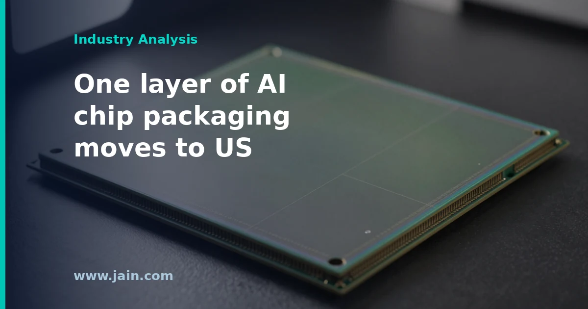
The part is a silicon “interposer”: a thin slab of silicon that sits under an artificial intelligence processor and wires it to its memory, like a shared floor both chips are mounted on. The packaging step built around it has been one of the main limits on how many artificial intelligence chips get shipped.
Making it in America could add supply outside Taiwan. But it covers one step, not the whole chip.
Yahoo Finance reported that GlobalFoundries and TSMC have reached a $2 billion deal for silicon interposers produced in the United States. Silicon interposers are the base layer in the advanced packages that join high-end AI processors to stacked high-bandwidth memory, which places the agreement inside the part of the GPU supply chain that has repeatedly constrained output.
The deal follows TSMC’s October 8 Form 6-K, its September 2026 revenue report, which showed consolidated revenue of roughly NT$511.86 billion for the month, up 54.6 percent from September 2025, and NT$3,898.73 billion for January through September, up 41.1 percent year over year.
Executive Summary
The headline facts are simple: a $2 billion agreement between the world’s largest contract chipmaker and a US-headquartered specialty foundry, covering a component that is made in the United States. The interposer is not a commodity part. It is a large piece of silicon, patterned in a wafer fab with fine wiring and vertical connections called through-silicon vias. AI accelerators mount their compute die and memory stacks on it side by side.
That matters because AI chip supply has been gated less by the ability to make processors than by the ability to package them with memory. Making interposers in the US adds a domestic source for one input to that packaging flow. However, an interposer is an intermediate part. Until the companies say where the rest of the package is assembled, the deal shows where part of the bottleneck can be relieved, not that it has been.
For GlobalFoundries, a $2 billion commitment tied to AI packaging is a significant new line for a foundry that stepped back from the leading-edge process race in 2018. For TSMC, whose September revenue alone was more than NT$500 billion, the deal is small in financial terms. Its importance is geographic and logistical.
Why the Interposer Sits on AI’s Critical Path
The most capable AI accelerators are not a single chip. They are assemblies. A large processor die sits next to several stacks of high-bandwidth memory (HBM), DRAM chips stacked vertically to deliver very fast data access. These parts have to talk to each other across thousands of extremely fine connections, far denser than an ordinary circuit board can carry. The silicon interposer solves this. It is a slab of silicon wired with lithography, the same patterning process used to make chips, so the processor and memory can be packed millimetres apart and connected at chip-level density.
TSMC’s version of this approach is CoWoS, short for chip-on-wafer-on-substrate. Dies are bonded onto an interposer wafer, which is then mounted on a conventional package substrate. In recent years, CoWoS capacity has been widely identified as a binding constraint on AI accelerator shipments. The processors could be fabricated, but there was not enough capacity to package them with their memory. Interposers are one input to that flow. Because they are made in a fab rather than an assembly house, adding interposer supply requires wafer capacity with the right tooling, not just more packaging lines.
What Onshoring One Layer Does, and What It Doesn’t
This is the substance behind the headline. A US-based interposer source moves one fab-made step of AI packaging onto American soil. That has real value. It adds a source outside Taiwan for a component tied to a known chokepoint. It suits a mature, non-leading-edge process, which plays to GlobalFoundries’ strengths in its New York and Vermont fabs. It also gives chip designers and their hyperscale customers, the largest cloud and AI operators, a domestic option to cite when they are asked about supply resilience.
But an interposer alone does not make a finished accelerator. After the interposer is made, the processor dies and memory stacks must be bonded onto it. The assembly must then be mounted on a substrate, tested, and shipped. If those steps remain in Taiwan, US-made interposers simply cross the Pacific in the opposite direction from the processors. Much of the processor output from TSMC’s Arizona fabs has itself needed to return to Taiwan for advanced packaging. The deal becomes a genuinely domestic AI supply chain only when it pairs with US assembly capacity. TSMC said in March 2025 that its expanded Arizona plans include advanced packaging facilities, and its October 6-K shows continued financial support for US subsidiaries, recording lending to TSMC Washington and guarantees for TSMC Arizona. Connecting the interposer supply to that assembly capacity is the step that would turn a single onshored layer into an onshored package.
The packaging variant also matters. TSMC’s family includes the original CoWoS-S, which uses a full silicon interposer, and newer variants such as CoWoS-L, which replace the full interposer with smaller embedded silicon bridges. If flagship accelerators continue shifting toward bridge-based designs, the market for full-size interposers looks different. Which products these US interposers serve will determine how much of the bottleneck they actually touch.
Reading $2 Billion Against Each Company’s Scale
For TSMC, the figure is modest. Its September revenue was about NT$511.86 billion, and its year-to-date revenue was NT$3,898.73 billion, up 41.1 percent. A $2 billion agreement is not a material financial event at that scale. It is a capacity and location decision. Choosing a domestic partner for a mature-process component frees TSMC to focus its own capital elsewhere while adding a US element to its packaging chain.
For GlobalFoundries, the calculus runs the other way. A foundry that chose in 2018 to stop pursuing the most advanced process nodes now has a direct line into the most supply-constrained segment of the AI hardware market, using processes it already runs. That makes it a significant win, though its annual revenue impact cannot be assessed until the contract’s duration and ramp are known. The two companies were once adversaries in a patent dispute that they settled in 2019 with a broad cross-license. A supply relationship on AI packaging is a notable evolution from that history.
Background
TSMC, founded in Taiwan in 1987, is the world’s largest contract chipmaker. It manufactures processors for most leading AI chip designers, and its CoWoS packaging has become central to AI accelerator supply. It is building fabs in Arizona and has said its US plans include advanced packaging. GlobalFoundries, spun out of AMD in 2009, runs fabs in Malta, New York; Essex Junction, Vermont; Dresden; and Singapore. It stopped pursuing the most advanced process nodes in 2018 to focus on specialty technologies.
The two companies settled a patent dispute in 2019 with a broad cross-license. Their new interposer agreement places GlobalFoundries’ US mature-process capacity inside the AI packaging flow that TSMC dominates.
The chips that run artificial intelligence are not held up by the factories that print them. They are held up by the assembly step at the end, where a processor and its memory are bonded onto a single slab so they can talk to each other fast enough.
Taiwan Semiconductor Manufacturing Company owns most of the world’s capacity for that step. Analysts in Taiwan say it plans to roughly double that capacity by 2028. Until it does, anyone building an artificial intelligence data center is standing in a queue. Intel is selling a rival method, and smaller assembly firms are absorbing the overflow.
Wccftech, citing a Taiwanese media report that quotes analysts, said TSMC plans to expand its chip-on-wafer-on-substrate (CoWoS) advanced packaging capacity to 260,000 wafers per month by the end of 2028, roughly double the approximately 130,000 wafers per month the same forecast puts it at by the end of 2026. The expansion is said to center on TSMC’s Arizona campus and its AP7 packaging facility in Taiwan.
The same forecast estimates that Intel’s competing EMIB-T packaging, converted into CoWoS-equivalent 12-inch wafer terms, could reach 15,000 to 20,000 wafers per month in 2027 and 40,000 to 45,000 in 2028, and says the CoWoS shortage has pushed work toward other packaging firms including Amkor, UMC and ASE. TSMC has not published a capacity target of its own. In a Form 6-K filed with the Securities and Exchange Commission on September 10, the company reported August 2026 consolidated revenue of NT$514.81 billion, up 53.3 percent from a year earlier.
Executive Summary
Advanced packaging is the step where a logic die and its stacks of high-bandwidth memory are mounted together onto a shared substrate so they behave as one component. CoWoS is TSMC’s version, and it is the packaging used for the accelerators that fill AI data centers. For roughly three years it, rather than leading-edge wafer manufacturing, has been the narrowest point in the supply chain for those parts.
A doubling of that capacity by 2028 would be the single largest change to AI hardware availability that any one company can make. It would not, however, double accelerator output in a straight line. Package sizes are growing, the newest designs consume more interposer area and more memory stacks per unit, and a wafer of packaging substrate therefore yields fewer finished accelerators each generation than it did the year before. Capacity that doubles against demand that also rises per unit is not the same as supply that doubles.
TSMC’s own disclosure does not address packaging capacity. What its September 10 filing does show is demand running hot: August revenue rose 53.3 percent year over year, and revenue for the first eight months of 2026 was up 39.3 percent. That is consistent with a company selling everything it can finish, which is the condition under which a capacity forecast of this kind becomes credible without being confirmed.
The Bottleneck Moved Downstream
For most of the history of the chip industry, the scarce resource was the front end: photolithography tools, leading-edge wafer starts, yield on a new process node. Packaging was the cheap, unglamorous back end. AI accelerators inverted that. A modern accelerator is not one chip but an assembly, a large logic die surrounded by stacks of memory, all sitting on a silicon interposer threaded with vertical connections called through-silicon vias. The density of those connections is what delivers the memory bandwidth the workload needs. That assembly step is CoWoS, and there is no abundant substitute for it.
The practical consequence for anyone financing a data center is that wafer capacity is no longer the number to watch. A foundry can start more wafers than it can finish into packages, and unfinished silicon does not train models. The forecast of 130,000 wafers per month at the end of 2026 rising to 260,000 by the end of 2028 is, in effect, a two-year schedule for how quickly the industry can convert build-ready halls into loaded racks.
Read it with care, though. Interposer area per accelerator has been climbing with every generation as designers add memory stacks and reticle-stitched logic. If the average package consumes meaningfully more of a wafer in 2028 than it does today, unit output grows by considerably less than the wafer count suggests. Doubling the input is a ceiling on supply growth, not a promise of it.
Arizona Can Print the Chips but Cannot Finish Them
The most operationally interesting detail in the forecast is geographic. Wafers produced at TSMC’s Arizona campus are flown to Taiwan to be packaged, because the packaging capacity sits on the island. Siting part of the expansion in Arizona alongside the AP7 facility in Taiwan would begin to close that loop, turning an American fab from a wafer source into something closer to a finished-component source.
That matters for reasons beyond logistics. A round trip across the Pacific adds days of cycle time and a customs and freight cost to every high-value wafer, and it means that the resilience argument for building fabs outside Taiwan is currently incomplete. A domestic fab whose output must still transit Taiwan to become a usable product does not remove the concentration risk that justified it. TSMC’s own filing shows the Arizona entity is treated as a significant subsidiary, with parent guarantees extended to TSMC Arizona among other affiliates, but the filing says nothing about packaging there.
For data center operators and the governments underwriting them, this is the question worth asking of any onshoring announcement: does the site produce a wafer or a shippable part? Until packaging follows fabrication, the answer for Arizona remains the former.
Intel’s EMIB-T and the Value of a Second Source
Intel’s EMIB-T takes a different architectural route. Instead of building the whole assembly on a large silicon interposer, it embeds small silicon bridges inside the organic substrate and places the logic and memory dies on top. Less silicon is used, which can mean lower cost and fewer of the handling and warpage problems that come with very large interposers, but the approach historically trades away some of the interconnect density that the largest, most bandwidth-hungry designs demand.
The forecast puts EMIB-T at 40,000 to 45,000 CoWoS-equivalent wafers per month by 2028. Against 260,000, that is a meaningful second source rather than a competitive threat, on the order of a sixth of the leader’s volume. The claim that it suits custom accelerators of the kind Google and Amazon design is plausible on architecture, since in-house cloud silicon is generally tuned for a known workload and a known cost target rather than for maximum bandwidth per package. It is also unverified: neither Intel nor any cloud provider has announced such an arrangement.
The spillover to Amkor, UMC and ASE follows the same logic. When the preferred supplier is sold out, work migrates to whoever can perform an adjacent version of it, and outsourced assembly and test firms have been the natural landing place. Buyers get optionality and a check on pricing. The risk is that second-source packaging is not a drop-in substitute. Requalifying a part on a different packaging architecture is an engineering program, not a purchase order, and the customers best placed to do it are the ones designing their own silicon.
What Is Substantiated and What Is Not
The demand side of this story rests on disclosed figures. TSMC’s September 10 filing with the Securities and Exchange Commission reports August consolidated revenue of NT$514.81 billion, a 10.1 percent increase on July and 53.3 percent on August 2025, with the first eight months of 2026 up 39.3 percent year over year. Growth at that rate at TSMC’s scale is difficult to explain without sustained AI accelerator demand behind it.
The supply side is a forecast, not a commitment. The 260,000 figure, the 130,000 baseline, the Arizona and AP7 split and the EMIB-T range all come from analysts rather than from the companies. None of the three firms named has published a packaging capacity target, a capital budget attached to one, or a schedule. Analyst capacity models in this industry have a reasonable track record on direction and a poorer one on timing, because packaging expansions depend on tool delivery, cleanroom construction and qualification cycles that slip quietly.
The sober reading is that the direction is well supported and the magnitude is an estimate. Treat 2028 as the earliest plausible date for materially looser accelerator supply, treat the doubling as a ceiling rather than a plan of record, and treat any procurement model that assumes it as carrying schedule risk that TSMC has not underwritten.
Background
TSMC is the world’s largest contract chip manufacturer, building processors designed by other companies. It commercialised CoWoS in the 2010s as a niche technique for high-performance parts, long before AI accelerators turned it into the scarcest resource in the industry. Today the packaging step determines how many finished accelerators reach the market, because a logic die without its memory bonded alongside it is not a usable product.
The competitive response has come from two directions. Intel has pushed its own bridge-based packaging as part of its foundry ambitions, targeting customers who want a supplier outside Taiwan or a lower-cost assembly for custom silicon. Outsourced assembly and test firms such as Amkor, ASE and UMC have absorbed work that TSMC cannot schedule. None of this has yet changed the basic shape of the market, in which one company’s packaging line sets the pace at which AI data centers can be filled.
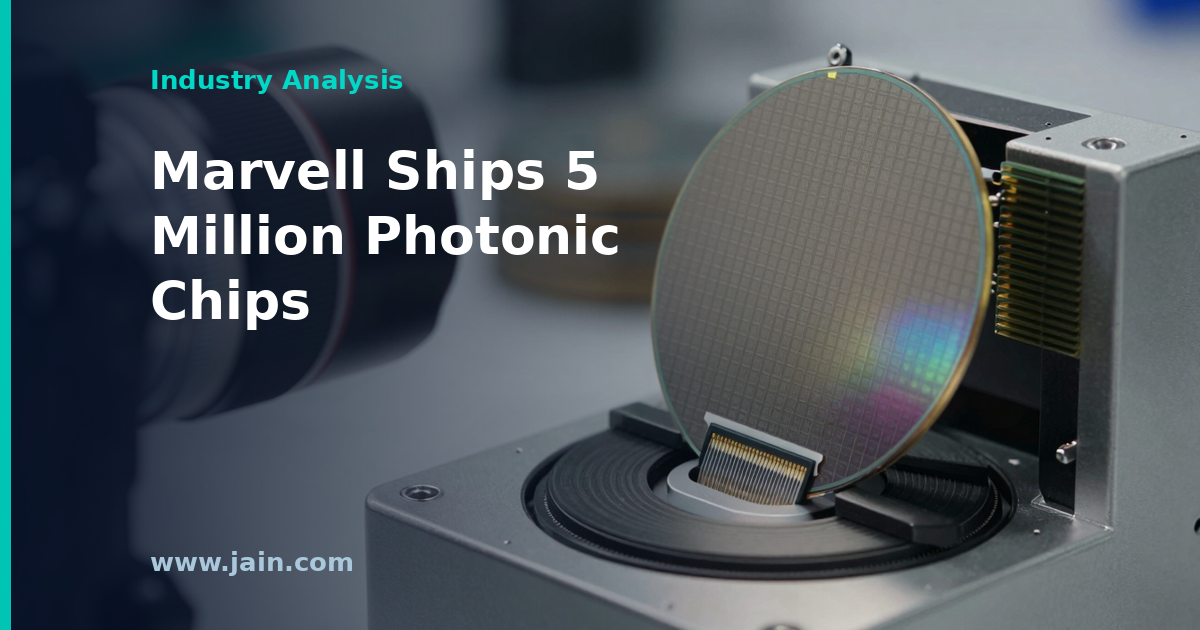
Marvell makes chips that move data using light instead of electricity. The company says it has shipped more than five million of them, built with a manufacturing partner, Tower Semiconductor.
That matters because the computers behind artificial intelligence are now so large they no longer fit in one room. Moving data between them fast enough has become a bottleneck, and light is the fix.
Marvell’s most recent quarter set a company revenue record: $2.739 billion, up 37 percent from a year earlier.
Stocktwits reported on June 18, 2026 that Marvell Technology (NASDAQ: MRVL) said it had shipped more than 5 million coherent photonic integrated circuits to customers worldwide, produced in partnership with specialty foundry Tower Semiconductor, and that Marvell shares rose more than 5% in premarket trading; the same report said the announcement came days before Marvell’s June 22, 2026 entry into the S&P 500, replacing Pool Corporation, and cited Nvidia chief executive Jensen Huang’s earlier description of Marvell as the “next trillion-dollar company.”
The company framed the shipment as a response to component scarcity in the data center market. “This milestone demonstrates the strength of our collaboration,” said Dr. Radha Nagarajan, Marvell’s Senior Vice President and Chief Technology Officer, Optical Engineering, adding that the two companies would “continue working… to advance next-generation coherent technologies for scale across data center architectures.” Two months later, in results reported to the SEC on August 27, Marvell posted record quarterly revenue of $2.739 billion, up 37% year over year, with Data Center revenue growth accelerating to 46%.
Executive Summary
A coherent photonic integrated circuit is a chip that sends and receives information as light rather than as electrical current, encoding data in the phase and amplitude of a laser beam. The technique was developed for long-haul telecom, where signals travel hundreds of kilometres. It has migrated into the data center because AI training and inference clusters have outgrown single buildings, and copper cabling loses too much signal over the distances involved.
The significance of a five-million-unit figure is not technical but industrial. Performance claims are made with a single working part; volume claims require yield, tested wafer capacity, packaging, and a foundry relationship that holds under load. Marvell attaching a unit count to a photonics announcement, rather than a data rate or a power-per-bit number, is a statement that this product line has left the qualification stage.
Marvell’s own financial disclosures give that claim a supportive backdrop without confirming its specifics. In the press release filed as an exhibit to its August 27 Form 8-K, Marvell reported record second-quarter fiscal 2027 revenue of $2.739 billion and guided the current quarter to $3.150 billion, plus or minus 5%. Chairman and CEO Matt Murphy pointed to “strong demand in Connectivity and a significant acceleration in our Custom business.” What the release does not do is size the photonics business itself.
A Unit Count Is a Supply Claim, Not a Speed Claim
Optical interconnect vendors usually announce firsts: the first 800-gigabit module, the first demonstration at a new modulation scheme. Those announcements tell buyers what is possible. A shipment total tells them something different and, for anyone building capacity, more useful — that parts exist in quantity, that they have been through a customer’s qualification process, and that a supplier is willing to be measured against a number it will have to keep growing.
That distinction is the heart of the story. For most of the current AI buildout, optics has been discussed as a constraint: lasers, modulators and the specialty processes that produce them have been among the harder items to source, alongside advanced packaging and memory. A supplier publicly counting units in the millions is signalling that at least one part of that constraint is loosening. It also changes the competitive question from who has the best device to who can produce devices reliably at a price that survives volume, which is the question commodities are settled on.
Buyers should hold the enthusiasm in proportion. The milestone is cumulative and undated — five million units shipped over what period, across how many product generations, and to how many customers are all open. A number that large spread thinly across several years and several generations describes a mature product family; the same number concentrated in recent quarters would describe a genuine volume inflection. Marvell has not said which it is.
The Foundry Half Deserves Equal Billing
Silicon photonics is a specialty manufacturing problem before it is a design problem. Building waveguides, modulators and detectors alongside conventional transistors requires process steps that leading-edge logic foundries generally do not offer, which is why the work concentrates in a small number of specialty fabs. Naming Tower Semiconductor in the announcement is therefore not courtesy — it identifies where the physical capacity actually sits.
This is a real strategic asset and a real dependency at the same time. A designer with a proven, high-yielding photonics platform at a partner fab has a lead that competitors cannot close by hiring engineers alone; process qualification takes years. But the same relationship concentrates risk. If demand for coherent optics keeps compounding at the rate Marvell’s Data Center commentary implies, the binding constraint moves upstream to wafer starts, laser supply and packaging throughput — none of which Marvell controls outright.
Neither company has described the commercial architecture underneath the partnership: whether capacity is contractually reserved, whether the arrangement is exclusive in either direction, or what expansion is planned. Those terms determine how much of a five-million-unit milestone is a durable moat and how much is a snapshot of a good year.
What the August Filings Confirm — and What They Leave Out
Marvell’s fiscal calendar ends in late January, so the quarter reported on August 27 (fiscal Q2 2027) covers the three months to August 1, 2026 — the period immediately following the photonics announcement. The results were strong on their face: revenue of $2.739 billion came in $39.0 million above the midpoint of prior guidance, GAAP net income was $308.0 million ($0.33 per diluted share), non-GAAP net income was $865.9 million ($0.94), and operating cash flow was $605.5 million. The company raised its revenue outlook for both fiscal 2027 and fiscal 2028.
The gap between $0.33 GAAP and $0.94 non-GAAP earnings is worth explaining rather than glossing over. GAAP figures follow standard accounting rules; Marvell’s non-GAAP measures exclude stock-based compensation, amortisation of intangible assets acquired in past deals, restructuring and similar items. The company itself notes in the release that acquired intangibles “contributed to Marvell’s revenues” and that their amortisation will recur. Both numbers are informative; neither is the whole picture, and the spread between them is unusually wide.
Crucially, the results tell you nothing directly about photonics. Marvell’s quarterly filings group revenue into Data Center and Communications and Other, and the 10-Q filed August 28 for the quarter ended August 1 also flags geographic revenue concentration, including China — a disclosure that matters for any company whose growth depends on globally distributed AI buildouts. Optical connectivity, custom AI silicon, storage and networking all sit inside the Data Center line. When management says growth accelerated to 46% there and that Custom will accelerate significantly in the second half, it is describing a portfolio, not a product. Anyone using the five-million-unit figure to infer photonics revenue is doing arithmetic the company has not enabled.
Index Inclusion and Endorsements Are Not Operating Results
Marvell’s addition to the S&P 500 generates mechanical demand for its shares from index funds, and it reflects that the company already met the index’s size, liquidity and profitability tests. It is a consequence of prior performance, not a cause of future performance, and it says nothing about coherent optics volumes, gross margin or customer concentration. The same holds for a competitor chief executive’s public praise: a warm comment from Nvidia’s Jensen Huang is a read on sentiment within the industry, not a purchase order, a forecast, or a commitment by anyone.
The more meaningful signal in the same window is the one attached to a filing. Raising the revenue outlook for two consecutive fiscal years in an SEC-furnished release carries legal weight that a milestone press release does not, because guidance is measured against actuals ninety days later. Marvell’s Q3 guide of $3.150 billion, with non-GAAP gross margin of 57.5% to 58.5% — slightly below the 58.9% just delivered — is the kind of detail that rewards attention: it implies a mix shift toward products that carry lower margin as they scale, which is exactly what commoditisation looks like in the numbers.
For infrastructure buyers, that trade is generally welcome. Falling unit economics on optical interconnect is how link budgets across a campus stop being a scarce resource. For investors, it is the tension to watch across Marvell’s October 6, 2026 Investor Day: revenue growing faster while the margin profile of the growth is not identical to the margin profile of the past.
Background
Marvell Technology is a Santa Clara-based supplier of data infrastructure semiconductors — the silicon behind networking, storage, custom accelerators and optical connectivity rather than the general-purpose processors most consumers recognise. Its optical position was substantially built through the 2021 acquisition of Inphi, which brought the digital signal processing expertise that turns raw optical signals into usable data links. The company’s fiscal year ends in late January, so its fiscal 2027 second quarter closed on August 1, 2026.
Tower Semiconductor is a specialty foundry that manufactures analog, radio-frequency and silicon photonics devices on processes distinct from leading-edge digital logic. Silicon photonics has spent two decades moving from telecom long-haul networks toward shorter reaches, and the AI buildout accelerated that migration sharply: as training clusters spread across multiple halls and campuses, the interconnect between them became a design constraint on how large a single computing fabric can be. That is the market both companies are addressing.