Applied Materials, one of the biggest makers of the machines that build computer chips, is buying more of a smaller Dutch company called Besi. It will own about a fifth of it.
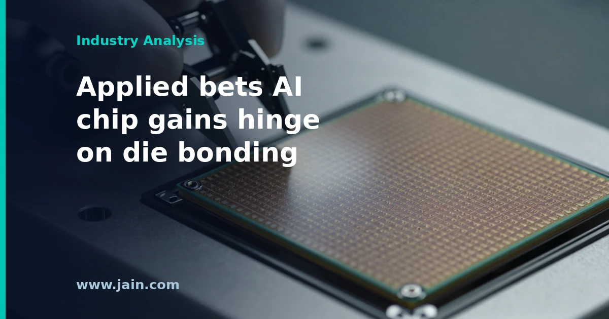
Besi makes machines that join separate chips together so they work as one. The most powerful artificial intelligence chips are now built this way, with stacks of memory chips placed right beside the processor.
The bet: the next big gains in speed and energy savings will come not just from making chips smaller, but from how tightly the pieces are joined.
Applied Materials (Nasdaq: AMAT) entered into an accelerated share purchase agreement on October 26, 2026 that, combined with its existing holding, would give it approximately 20% of the outstanding shares of BE Semiconductor Industries N.V. (Besi), the Amsterdam-listed maker of chip assembly equipment. In an 8-K filed the same day, Applied said delivery of the shares is subject to the expiration or termination of the waiting period under the Hart-Scott-Rodino Act, the US antitrust pre-merger review. Applied has not disclosed the price or number of shares.
MarketScreener reported that Besi’s shares soared on the news and described the move as roughly doubling Applied’s stake, which the company first took in April 2025. Applied said it views the investment as long term, has no current intention to go beyond about 20%, and will not seek a seat on Besi’s board.
Executive Summary
The world’s largest supplier of wafer-fabrication equipment is deepening its financial tie to the leading specialist in hybrid bonding, a technique that fuses chips together copper-to-copper without solder. Applied’s announcement frames the purchase explicitly around AI: Dr. Prabu Raja, President of Applied’s Semiconductor Products Group, said hybrid bonding and next-generation interconnect architectures are becoming “increasingly critical enablers of energy-efficient AI compute performance.”
The collaboration, which began in 2020, is also widening. Besi has joined Applied’s EPIC Center as an Innovation Partner, and joint work now extends beyond hybrid bonding into 3D chip stacking, logic and memory integration, thermo-compression bonding, and die-on-wafer, die-on-die and die-on-panel platforms. That list maps closely onto how today’s AI accelerators and their high-bandwidth memory are assembled.
The structure matters as much as the size. A capped 20% stake with no board representation gives Applied a large economic interest in Besi’s success without control over a supplier that much of the industry relies on.
Why Applied Is Betting on the Bond, Not Just the Transistor
A modern AI accelerator is rarely one piece of silicon. It is a package: one or more logic dies that do the computing, surrounded by stacks of high-bandwidth memory (HBM), the vertically stacked DRAM that feeds data to the processor. Performance and power draw depend heavily on how fast and how cheaply data moves between those pieces. Every connection between dies costs energy, and the number of connections that can be packed into a given area limits bandwidth.
Hybrid bonding attacks that limit directly. Instead of joining dies with tiny solder bumps, it presses two extremely flat, clean surfaces together so their copper pads fuse. That permits far denser connections at shorter distances, which is why Applied ties it specifically to “energy-efficient AI compute performance” rather than raw speed alone. The joint work list in Applied’s announcement, including logic and memory integration and next-generation 3D IC scaling, is a description of exactly this problem: getting memory and compute closer together.
Who feels this first: chipmakers designing multi-die AI processors, memory makers moving toward taller HBM stacks, and the packaging operations that assemble them. A front-end toolmaker taking a fifth of the leading bonding specialist is a strong signal that Applied expects interconnect density to be a gating factor in AI chip roadmaps, and that it wants a stake in whichever tools solve it.
Front-End Precision Meets Back-End Placement
The pairing makes technical sense. Hybrid bonding blurs the old line between front-end fabrication, where Applied built its business in deposition, etching and polishing, and back-end assembly, where Besi specialises in placing dies with high accuracy. A bond only works if surfaces are polished nearly atomically flat and kept free of particles, which are front-end disciplines, and if dies are then aligned and placed precisely, which is Besi’s.
Notably, the collaboration also covers the scaling of thermo-compression bonding, the incumbent method that uses heat and pressure on micro-bumps. That reads as a hedge on timing: the partners are positioned for the current generation of stacked memory and logic as well as the hybrid-bonded generation Applied describes as increasingly critical. Adding die-on-panel integration, which uses large rectangular panels instead of round wafers, extends the bet to a format the industry is exploring to fit more silicon into a single package.
A Stake, Not a Takeover
Applied was explicit on limits: approximately 20%, no current intention to go higher, no board seat, a long-term view. That restraint is meaningful. Besi sells to chipmakers and packaging houses that compete with one another, and equipment buyers tend to value suppliers that remain independent. A minority position without governance rights lets Applied share in Besi’s upside and coordinate engineering closely while Besi continues to sell to the whole market.
The mechanics add one caveat. Under an accelerated share purchase agreement, shares are acquired on a compressed timetable, but delivery here waits on the Hart-Scott-Rodino review. Until that clears, the agreement is signed but the stake is not yet delivered. Investors’ reaction suggests the market reads the move as validation of Besi’s technology position, though Applied’s statements stop short of any commercial commitment such as joint product revenue or guaranteed orders.
Background
Applied Materials, based in Santa Clara, California, is a leading supplier of the equipment used to make chips on silicon wafers, including tools for depositing, etching and polishing thin layers of material. As AI chips have shifted from single large dies to packages that combine several dies with stacked memory, advanced packaging has become a growing focus for front-end toolmakers.
Besi, headquartered in the Netherlands, built its business on die attach and packaging equipment and has become closely associated with hybrid bonding. The two companies began collaborating in 2020, Applied took an initial equity stake in April 2025, and Besi has since joined Applied’s EPIC Center as an Innovation Partner.
Intel, the American chipmaker, is expanding its research at a $5 billion lab in Silicon Valley run by Applied Materials, the company that builds the machines used to make computer chips.
The twist: Intel’s biggest rival in making chips for other companies, Taiwan Semiconductor Manufacturing Company, signed on to the same lab earlier this year. Two fierce competitors will be inventing future chips under one roof.
Why it matters: the chips behind artificial intelligence keep getting harder to make, and more of that early invention now happens at the machine maker, not inside any one chip company.
shattered.io reported that Applied Materials and Intel announced on October 6, 2026 an expanded collaboration on next-generation transistors, interconnects and advanced packaging, centered on Applied’s EPIC Center in Silicon Valley and Intel’s research campus in Hillsboro, Oregon. The work explicitly includes Foveros, Intel’s technology for stacking chip components vertically.
The EPIC Center, first pledged in May 2023 as an investment of up to $4 billion, is now described as a $5 billion facility. TSMC was confirmed as a founding partner in May 2026, five months before Intel’s expanded role was announced. No dollar figure, node target or performance goal was attached to the Intel agreement.
Executive Summary
Applied Materials, whose equipment sits inside virtually every leading-edge chip factory, now counts the two most closely watched advanced logic foundries (contract chip manufacturers) as research partners at the same facility. Intel’s expanded role covers the full stack of problems that limit AI processors: the transistors themselves, the microscopic wiring that connects them, and the packaging that joins multiple chip pieces into one product.
Intel CEO Lip-Bu Tan tied the work directly to AI demand, citing the need for gains in performance, power efficiency and packaging, and described Applied as an important partner in moving new technology from the lab into high-volume manufacturing in the United States. Intel Foundry’s chief technology and operations officer, Naga Chandrasekaran, framed faster R&D as critical to keeping pace with AI infrastructure buildout.
The significance lies less in any single deliverable, since none was disclosed, than in where the work is happening. When rival foundries both co-develop processes inside a toolmaker’s lab, the equipment vendor becomes a shared starting point for next-generation AI silicon.
Why the Toolmaker’s Lab Is Becoming the Starting Line
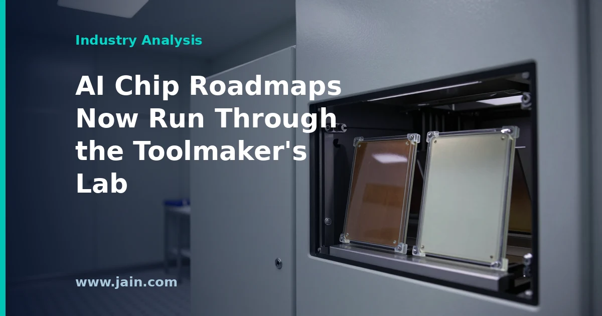
New chip generations do not begin at the factory. They begin with materials and process experiments: which film to deposit, how to etch a structure a few atoms wide, how to bond two pieces of silicon face to face. Those experiments depend on the equipment that will eventually run in production, which is why chipmakers co-develop processes with toolmakers. The EPIC Center, short for Equipment and Process Innovation and Commercialization, was built to formalize that step, with more than 180,000 square feet of cleanroom (ultra-clean manufacturing space) planned and up to 2,000 engineering jobs.
The scope of the Intel work maps onto the three constraints that matter most for AI processors. Front-end-of-line research targets the transistor layer. Back-end-of-line research targets interconnects, the wiring stacked above the transistors, where electrical resistance grows as features shrink and can become a bigger limit on speed and power than the transistors themselves. Packaging research, including Intel’s Foveros 3D stacking of chiplets (smaller dies combined into one package), targets interconnect density, power delivery and heat, all of which limit how much compute can be packed into an AI accelerator.
With TSMC as a founding partner and Intel as an expanded partner, at least part of the early-stage work on both companies’ next-generation AI silicon now passes through the same equipment vendor’s facility. That does not mean the two share designs or results; it means the toolmaker sees, and helps shape, both roadmaps. For AI chip designers who buy foundry capacity, it suggests that the process innovations available to them will increasingly be co-developed with Applied rather than invented in isolation inside one foundry.
Intel’s Math: A $2.1 Billion Loss and a Need for Outside Customers
Intel Foundry, the division that manufactures chips for Intel and outside customers, posted $5.8 billion in revenue and a $2.1 billion operating loss in its most recently reported quarter, a $348 million improvement on the prior period. Intel has raised its 2026 capital spending guidance to more than $20 billion company-wide, citing stronger customer-demand signals.
The division’s path to profitability runs through external customers, and winning them requires showing that Intel’s advanced nodes and packaging can match TSMC on schedule and yield. Intel says its 18A process has been in volume production in Arizona since December. Moving from a node that works to a node that wins outside AI chip business is where materials and packaging co-development pays off, and packaging is one area where Intel has distinctive technology to offer.
Neutral Ground Is Good Business for Applied
For Applied Materials, hosting both foundries reduces dependence on any single customer’s spending cycle. The company reported fiscal third-quarter 2026 revenue of $9.12 billion, with $7.04 billion coming from its Semiconductor Systems segment, which sells the equipment used for leading-edge manufacturing. Every process co-developed at EPIC is, in practice, a process that runs on Applied tools.
The facility’s cost has also grown: from a pledge of up to $4 billion over seven years in 2023 to a project now described as $5 billion. Cost growth is common in cleanroom-heavy construction, and anchor partners help justify it. The open question is how Applied manages confidentiality when two direct competitors work in the same building, a matter the companies have not addressed publicly.
A Shared Lab Does Not Close the Spending Gap
Shared research access can equalize the starting line for process experiments, but not manufacturing scale. TSMC has guided 2026 capital spending to $60 billion to $64 billion, up from roughly $56 billion, roughly three times Intel’s company-wide figure of more than $20 billion. Whoever converts lab results into high-volume production fastest still needs the factories to do it.
Samsung Foundry, the third major advanced-logic contender, has no confirmed role at the EPIC Center, and its foundry results are reported inside Samsung Electronics’ broader semiconductor segment. For buyers of AI silicon, the practical takeaway is that process and packaging advances developed at EPIC may reach both Intel and TSMC customers, while capacity remains the differentiator.
Background
Applied Materials is one of the world’s largest makers of semiconductor manufacturing equipment, the deposition, etching and inspection machines that chip factories use to build transistors and wiring. It unveiled the EPIC Center in May 2023, pledging up to $4 billion in incremental investment over seven years, more than 180,000 square feet of cleanroom space, up to 2,000 engineering jobs and as many as 1,500 construction jobs. The project is now described as a $5 billion facility and is scheduled to be operationally ready in 2026.
Intel Foundry is Intel’s contract-manufacturing division, built to produce chips for outside customers as well as Intel’s own products, in direct competition with TSMC, the world’s largest contract chipmaker. Intel CEO Lip-Bu Tan has positioned AI demand and US-based high-volume manufacturing as central to the foundry strategy.
The chips behind AI tools like chatbots are not just manufactured. They are also assembled: several chips are placed side by side or stacked, then wired together into one package. How well that assembly works now affects how fast new AI chips can ship.
TSMC, the Taiwanese company that makes many of the world’s AI chips, is building a center in southern Taiwan to test new assembly machines and materials before they reach the factory floor. The goal is to catch problems early, instead of fixing them while production is already running.
Do not expect quick results. The center is due to open in late 2029.
Kaohsiung’s Baipu Industrial Park broke ground on September 21, 2026. SemiVision reported that TSMC will anchor the park with an advanced-packaging training and validation center. The center is not a production line. It is a facility where TSMC and its suppliers will jointly develop, test and qualify packaging equipment and materials. Earlier plans put TSMC’s initial site at roughly three hectares with two buildings, and operations are expected to begin around the fourth quarter of 2029.
The park covers about 88.7 hectares, including roughly 53 hectares of industrial land. Around 25 hectares of that are expected to focus on advanced back-end semiconductor equipment and related supply chains. Official estimates suggest the park could eventually generate around NT$300 billion in annual output and more than 4,000 jobs.
Executive Summary
TSMC’s Baipu center is built around a reconfigurable “Mini-Loop” validation platform. It will not house a complete CoWoS production line. Instead, selected process modules will be assembled, tested and swapped out as technologies change. CoWoS (Chip-on-Wafer-on-Substrate) is TSMC’s technique for placing an AI processor next to stacks of high-bandwidth memory (HBM) inside a single package, and it sits at the core of today’s AI accelerators.
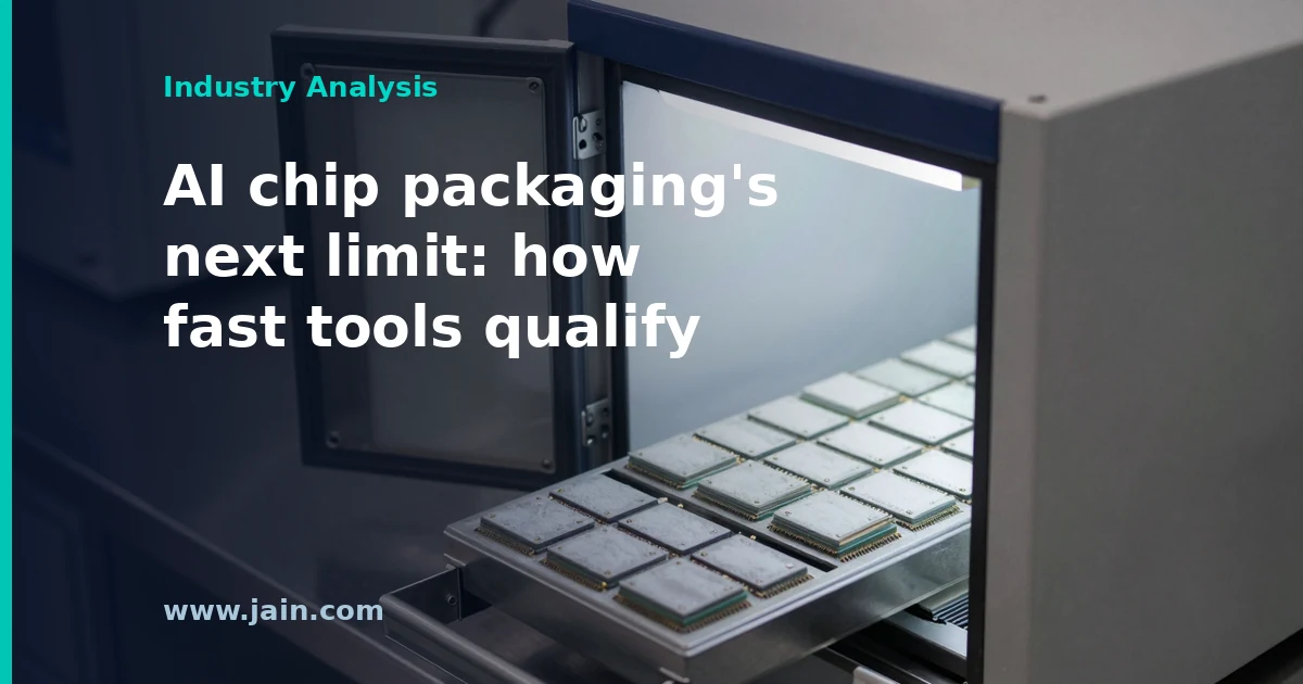
The significance lies in what TSMC is separating out. It is moving equipment and materials validation out of its production fabs and into a dedicated site shared with suppliers. Validation is the work of proving that a new tool or material performs reliably enough for mass production. The move is a bet that AI chip supply increasingly depends on how quickly new packaging tools and materials can be qualified, and not only on how many packaging lines exist.
For suppliers, the promise is earlier entry into TSMC’s development cycle. For AI chip designers, the payoff, if it comes, is fewer surprises when new package designs reach volume production. Neither benefit is expected before late 2029.
Why the Gating Step Is Qualification Time, Not Floor Space
Front-end chipmaking, the step where transistors are patterned onto wafers, relies on equipment giants such as ASML, Applied Materials, Lam Research and Tokyo Electron. These companies run large R&D organizations and global field-service teams that help get new tools qualified. Advanced packaging has no equivalent bench strength. Many back-end equipment suppliers are much smaller, yet a long list of technologies is changing at the same time:
CoWoS itself
Hybrid bonding, which fuses chips copper-to-copper without solder bumps
Thermocompression bonding (TCB)
Temporary bonding and debonding
Wafer and panel handling
Automated optical inspection and metrology
Underfill, dielectric and thermal materials
The product cadence on top of that is accelerating. NVIDIA, AMD, Broadcom and custom AI chip (ASIC) developers keep introducing new architectures. HBM is moving from HBM3E toward HBM4 and beyond. Package size, die count, interconnect density and heat load are all rising together. The practical result is that one generation of equipment may not finish qualification before the next product generation arrives. Historically, some packaging tools were still being modified after installation, with engineers tuning them while production was already underway. A line that is being debugged is not yielding at full rate.
Baipu is TSMC’s structural answer: move troubleshooting upstream, so that equipment, material and integration problems surface before mass production. This is why capacity counts alone understate the constraint. A packaging plant full of tools that are not yet qualified for the next package design cannot ship the next accelerator. Two groups are most exposed. The first is accelerator designers, whose launch timing depends on new package formats. The second is smaller back-end toolmakers, who have lacked a place to prove their equipment at the pace TSMC’s customers now demand.
The Mini-Loop Is a Capital-Efficiency Choice
A fixed, full-scale experimental packaging line would require heavy capital expenditure. Because 3D IC, CoWoS, HBM and chiplet architectures are evolving quickly, that line’s configuration could be outdated within a few years. The Mini-Loop concept avoids this. TSMC brings in only the module that needs validating, tests it, modifies it, and then reconfigures for the next job. The validation infrastructure evolves with each technology generation instead of being written off along with the previous one.
The trade-off is fidelity. A modular loop tests modules. Some integration problems only appear when every step runs together at volume, and those may still surface in production. How much time Baipu actually saves will depend on two things: how TSMC bridges that gap, and whether validation results at Baipu carry directly into production qualification or must be partly repeated in the fabs.
From Equipment Vendor to Co-Development Partner
The conventional sequence runs like this: the customer sets a specification, the supplier builds the tool, the tool is installed in the fab, qualification begins, and then the equipment is modified in response to feedback. Baipu aims to put customers, equipment makers, materials companies and research organizations into the same development loop before mass production begins. In that loop, equipment fixes can happen immediately, and materials can move straight into another design of experiments (DOE, a structured test matrix). Software, automation, process recipes and metrology can all be tuned in parallel.
This is a different advantage from simple proximity. Being near TSMC saves shipping and service time. Entering its development cycle early lets a supplier help shape the specification instead of chasing it. The groundbreaking drew companies from across the stack: TSMC, ASE, Foxconn, ASPEED, WinWay, King Slide, Gudeng, C SUN, Grand Process Technology, Scientech, AblePrint, HIWIN and Gallant Precision Machining. Attendance does not confirm investment. The first phase is expected to include validation work linked to TSMC and its suppliers, along with Foxconn AI-related R&D and manufacturing. A later phase could support further advanced-packaging expansion, including requirements from companies such as ASE.
Kaohsiung presents Baipu as one link in a southern-Taiwan corridor:
Nanzih: advanced semiconductor manufacturing
Renwu: packaging and test
Ciaotou: materials and critical components
Gangshan and Lujhu: existing precision-machinery, metal-processing and fastener industries that the city hopes to pull into the equipment supply chain
If that works, the regional advantage would not rest on any single fab. It would rest on how tightly manufacturing, packaging, equipment and qualification can iterate over short physical distances.
What a 2029 Opening Means for Today’s AI Supply
With operations expected around the fourth quarter of 2029, Baipu sits outside the window of current packaging constraints. Tools and materials qualified there would serve product generations well beyond today’s HBM3E-based parts. Buyers of AI accelerators should not read Baipu as near-term relief. It is an investment in the rate at which packaging technology can change over the following years.
The headline economic figures are NT$300 billion in annual output and more than 4,000 jobs. These are park-wide official estimates, not TSMC commitments, and they say little about the metric that matters most to the industry: how much shorter qualification cycles actually become. No such target has been published. The argument that time-to-qualification is becoming the gating factor is coherent and fits the direction of packaging technology. Its payoff, however, will only be measurable in how many Baipu-validated tools reach production lines at TSMC, ASE or other manufacturers.
Background
TSMC (Taiwan Semiconductor Manufacturing Company) manufactures chips designed by other companies. In the AI era, its role has extended from wafer fabrication into advanced packaging. Packaging is the step where multiple chips, such as a processor and stacks of high-bandwidth memory, are combined into a single package. Technologies such as CoWoS, hybrid bonding and 3D IC stacking have made packaging a performance-critical part of AI accelerators, and HBM, substrates, thermal management, metrology and automation have become increasingly interdependent.
Southern Taiwan is a focal point of that build-out. Kaohsiung’s semiconductor base already spans Nanzih, Renwu and Ciaotou. The city is positioning Baipu Industrial Park, which broke ground in September 2026, as both an advanced semiconductor equipment and materials validation hub and an AI advanced-manufacturing base.
Applied Materials builds the huge machines that factories use to make computer chips, including the chips that power artificial intelligence.
It plans to spend $5 billion in India over ten years, including a research campus bigger than 100 football fields.
The more interesting goal: making ten times as many of its machine parts in India by 2035, so fewer of them depend on a handful of places.
Investors liked it. The company’s shares climbed sharply the day the plan became public.
StocksToTrade reported that Applied Materials (Nasdaq: AMAT), one of the world’s largest makers of semiconductor manufacturing equipment, has unveiled a $5 billion expansion in India to be carried out over 10 years. The plan includes a 140-acre research and development campus and a tenfold increase in local supply chain capacity by 2035.
The shares closed at $444.65 on Friday, September 18, 2026, up from the low $420s earlier in the week. In the same week the company added Qualcomm’s chief financial officer and chief operating officer to its board.
Executive Summary
Applied Materials is committing $5 billion over a decade to India. The plan has two parts: a 140-acre R&D campus and a pledge to grow local supply chain capacity tenfold by 2035. The campus will draw the headlines. The supplier target is the more consequential part.
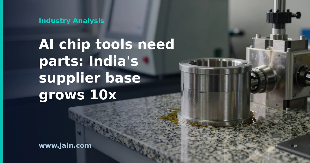
Chip-equipment makers such as Applied do not build every part of their machines themselves. Their deposition, etch and inspection tools are assembled from thousands of precision components made by outside suppliers. Those tools are in strong demand because of AI chip production. How fast Applied can ship depends partly on how deep and how geographically diverse its supplier base is. A tenfold expansion of Indian supply capacity is a bet on building a second source of those parts, outside the US-Taiwan corridor where much of the industry is concentrated today.
The spending is small next to Applied’s cash generation. The company reported roughly $2.33 billion of free cash flow and about $707 million of capital expenditure in its latest quarter. It also still has $12.8 billion authorised for share buybacks.
The Tenfold Target Matters More Than the Campus
A research campus shows commitment, but on its own it adds engineers rather than output. The tenfold increase in local supply chain capacity by 2035 is the operational commitment in this plan. Semiconductor equipment is built from many specialised parts: vacuum chambers, gas-delivery systems, precision-machined metal and ceramic components, and electronics. When chipmakers raise orders, as AI accelerator and memory demand has pushed them to, delivery times depend on the slowest supplier as much as on the tool maker’s own factories.
Multiplying Indian supply capacity gives Applied another place to source those parts. It also gives India’s precision-manufacturing firms a route into one of the most demanding supply chains in industry. The groups most directly affected are Indian component makers who can qualify to Applied’s standards and incumbent suppliers elsewhere who may face new competition. Chipmakers buying tools could also benefit if a broader supplier base eventually shortens or steadies lead times, although Applied has not said that is the aim.
A Pattern Beyond the US-Taiwan Axis
Applied is not the only large equipment maker expanding in India. Lam Research, a direct competitor in etch and deposition, has also set up manufacturing there. When two of the largest tool makers invest in the same country, it suggests the industry is treating India as a lasting part of its supply base rather than a one-off hedge.
The logic is resilience, not only cost. Much of advanced chipmaking capacity sits in Taiwan, and a large share of tool design and assembly sits in the United States. That concentration is a risk for anyone planning AI compute build-outs years ahead. Building supplier depth in a third region spreads that risk. The limit is time: 2035 is a long way off, and qualifying new suppliers for semiconductor-grade parts is slow and exacting work.
Easily Funded on Current Cash Flow
Spread evenly, $5 billion over 10 years comes to about $500 million a year. That is below Applied’s latest single-quarter capital spending of roughly $707 million and a fraction of its approximately $2.33 billion in quarterly free cash flow. The company reported quarterly revenue of $9.115 billion at a gross margin near 63.9%, with debt-to-equity around 0.29.
That means the India plan does not crowd out shareholder returns. Applied pays a $0.53 quarterly dividend, has raised it for nine straight years, and retains $12.8 billion in buyback authorisation. The more realistic constraint is execution, meaning hiring, supplier qualification and local infrastructure, rather than money.
What the Market Is and Is Not Pricing
Analysts are broadly positive but not unanimous on valuation. UBS raised its price target to $695 with a Buy rating, and the average target sits near $664. Mizuho cut its target to $590 while keeping an Outperform rating, citing pressure on sector valuation multiples and leaning on memory and DRAM equipment demand.
That split reflects a wider debate. Demand for AI chip equipment is strong now, but equipment makers are cyclical, and investors periodically question how long AI capital spending can keep rising. A 10-year India commitment is a statement that Applied is planning past any single cycle. The share-price reaction shows the market rewarded that signal before most of the details were known.
Background
Applied Materials is one of the largest suppliers of semiconductor manufacturing equipment. It sells to foundries, logic chipmakers and memory producers worldwide and trades on Nasdaq under AMAT. Its profitability is high for the sector, with a gross margin near 63.9% and quarterly revenue of about $9.1 billion.
Chip-equipment makers have enjoyed strong demand as AI drives investment in advanced logic and memory. The industry’s manufacturing and supplier base remains concentrated in a few regions, chiefly the United States and East Asia. India has been courting semiconductor investment, and competitors including Lam Research have already built operations there.
Lam Research does not make computer chips. It makes the machines that make them — room-sized tools that carve circuits into silicon wafers.
The company plans to spend about 1.1 billion dollars, or Rs 10,000 crore, on a manufacturing plant in India.
Why it matters: only a few places in the world build these machines, and a new chip factory can wait a long time for one. Every artificial intelligence data centre sits downstream of that wait. A new place to build the tools is a new way to shorten it.
INDIA New England News reported that Lam Research Corporation, one of the world’s largest makers of semiconductor manufacturing equipment, will invest Rs 10,000 crore — roughly $1.1 billion at current exchange rates — in a semiconductor manufacturing facility in India.
Lam is a wafer fabrication equipment (WFE) supplier rather than a chipmaker: its systems etch and deposit the microscopic layers that make up a finished chip, and they are bought by the logic foundries and memory manufacturers that supply the processors and high-bandwidth memory used in artificial intelligence hardware. The investment figure is the substantive disclosure in the announcement; site, phasing, product mix and start-up date were not specified.
Executive Summary
The headline number is large by the standards of India’s semiconductor programme and unusual in its position in the supply chain. Most of the country’s chip announcements to date have concerned fabrication and assembly-test-packaging plants — the places where chips are made and put into packages. An equipment plant sits one layer higher: it makes the capital tools that every fab, anywhere, has to buy before it can produce anything at all.
That distinction is why the commitment is worth attention beyond India. Advanced chip toolmaking is concentrated in a small number of countries — principally the United States, Japan, the Netherlands, and the Taiwan-Korea manufacturing corridor that absorbs much of the output. Lead times on advanced etch and deposition systems are measured in quarters, not weeks, and they are the practical constraint on how quickly a foundry or memory maker can convert a capital-expenditure announcement into shipping silicon.
For data centre operators, cloud providers and anyone financing artificial intelligence capacity, this is the least visible link in the chain and one of the least elastic. A second significant node of tool manufacturing does not solve that constraint on its own. It does change the geography of it — and geography is the variable that has driven the last four years of semiconductor industrial policy.
The Layer Above the Chip Shortage
Public conversation about semiconductor supply focuses on fabs: who is building one, where, and how many wafers it will start per month. The equipment layer above it gets far less attention despite being the gating item. A fab is, in economic terms, mostly a building full of tools. The cleanroom shell, the power feed and the ultrapure water plant are expensive and slow, but they are construction problems with known solutions. The etch chambers, deposition systems, lithography scanners and metrology tools inside are the scarce, long-lead, technically differentiated part.
Lam Research occupies two of the most important slots in that equipment stack. Etch is the subtractive step — selectively removing material to define features. Deposition is the additive step — laying down films sometimes only a few atoms thick. Both processes are repeated hundreds of times over the life of a single wafer, and both have become more tool-intensive as chipmakers moved from flat transistor designs to three-dimensional ones and from planar memory to stacked memory. More process steps means more tools per unit of output, which means equipment demand grows faster than wafer demand.
That structural point is what makes an equipment-manufacturing investment different from a fab investment. A fab serves its owner’s customers. An equipment plant serves everyone building fabs.
Why AI Capacity Waits on Tools, Not Just Fabs
Here is the mechanism the Rs 10,000 crore commitment plugs into. When a memory manufacturer decides to add high-bandwidth memory capacity — the stacked memory that sits alongside an artificial intelligence accelerator and largely determines how fast it can be fed data — it does not simply turn on a line. It places tool orders, waits out the manufacturer’s backlog, takes delivery, installs, qualifies, and only then ramps. The same sequence applies to a foundry adding advanced logic capacity. The interval between the capital decision and the first qualified wafer is dominated by equipment delivery and installation, not by construction.
That interval is what data centre operators experience, one or two steps removed, as accelerator allocation. An operator signing for capacity today is bidding against everyone else for chips whose production capacity was ordered as tools several quarters earlier. When equipment backlogs lengthen, the effect propagates downstream on a lag: tighter chip allocation, longer hardware delivery windows, and capacity plans that slip into the following year. It is a slow-moving constraint, which is exactly why it is easy to under-weight until it binds.
A roughly $1.1 billion manufacturing facility does not shorten that queue by itself, and nobody should claim it does. What it does is add manufacturing capacity and a new geography to a supply base that is unusually concentrated, in a country that is simultaneously trying to build the fabs that consume the output. The effect that matters for buyers is optionality — more places where tools, subsystems and spares can be built and shipped from, and one less single-region dependency in the layer that gates everything below it. Who benefits, concretely: chipmakers ramping capacity, whose tool delivery schedules set their ramp; and the operators and financiers downstream, whose capacity timelines inherit those schedules whether they track them or not.
What Rs 10,000 Crore Actually Buys
Even-handedly, the announcement establishes scale and intent, not capability. Semiconductor equipment plants span a wide range of activity, and the differences are material. At one end is manufacture of subsystems, modules, chambers and precision components, plus spares and refurbishment — genuinely valuable, high-employment work that improves supply resilience without relocating core technology. At the other is final assembly and test of complete process tools, which carries far more supply-chain weight. The announcement as reported does not say which of these the facility will do, or in what mix over time.
The realistic reading is that a plant of this size is a multi-year, phased build rather than a single switch-on, and that its early output is likelier to be components and subsystems than flagship systems. That is not a criticism; it is how equipment supply chains are normally localised. It does mean the supply-chain effect is gradual and should be judged over years, against disclosed milestones, rather than assumed from the headline figure.
There is also an ecosystem question underneath the capital number. Equipment manufacturing depends on a dense local base of precision machining, vacuum components, ultra-clean fabrication, specialty materials and calibrated metrology. India has been building toward that base, but a plant of this scale tends to pull suppliers with it rather than find them already in place. The supplier development timeline, not the construction timeline, is often what determines when a facility reaches meaningful local content.
India Moves Up the Stack, and Why That Is the Interesting Part
India’s semiconductor strategy has been read, sometimes dismissively, as a late entry into commodity fabrication and packaging. An equipment investment complicates that reading. Toolmaking is higher-margin, more engineering-intensive and considerably harder to replicate than assembly — and it is a market where demand comes from every fab on earth rather than from a domestic customer base that India is still building. A plant serving global equipment demand does not need local fabs to be viable, which removes the sequencing problem that has slowed other parts of the programme.
For the wider industry, the significance is directional rather than immediate. Since 2020, the semiconductor supply chain has been reorganised around resilience — second sources, allied manufacturing, and reduced exposure to any single strait, grid or jurisdiction. Most of that effort has gone into chips themselves. Far less has gone into the tools, which remain the narrowest part of the chain. Adding a manufacturing node in a fourth major jurisdiction is a modest structural change in the right direction, and it is the kind of change that shows up in lead-time statistics years after the ribbon-cutting, if it shows up at all.
The honest caveat is that concentration is not only about where plants sit. Intellectual property, critical subcomponents and the scarcest engineering talent can remain concentrated even as assembly disperses. Diversifying manufacturing footprint and diversifying the supply chain are related but not identical, and the announcement as it stands speaks to the first.
Background
Lam Research Corporation, headquartered in Fremont, California, is one of the small group of companies that supply the wafer fabrication equipment used by every advanced chip factory in the world. It is best known for etch and deposition systems and sells to both logic foundries and memory manufacturers. Its business is inherently cyclical: revenue tracks its customers’ capital spending, which rises and falls with chip demand — and which has been pushed upward in recent years by investment in capacity for artificial intelligence processors and the memory that accompanies them.
India launched a national semiconductor programme earlier this decade, pairing capital incentives with state-level support to attract fabrication, assembly and testing investment. Most announced projects to date have sat in those downstream segments. Equipment manufacturing is a newer and higher-margin part of the chain, and one where global demand does not depend on a domestic customer base — which is what makes an investment at this layer notable in the programme’s trajectory.