
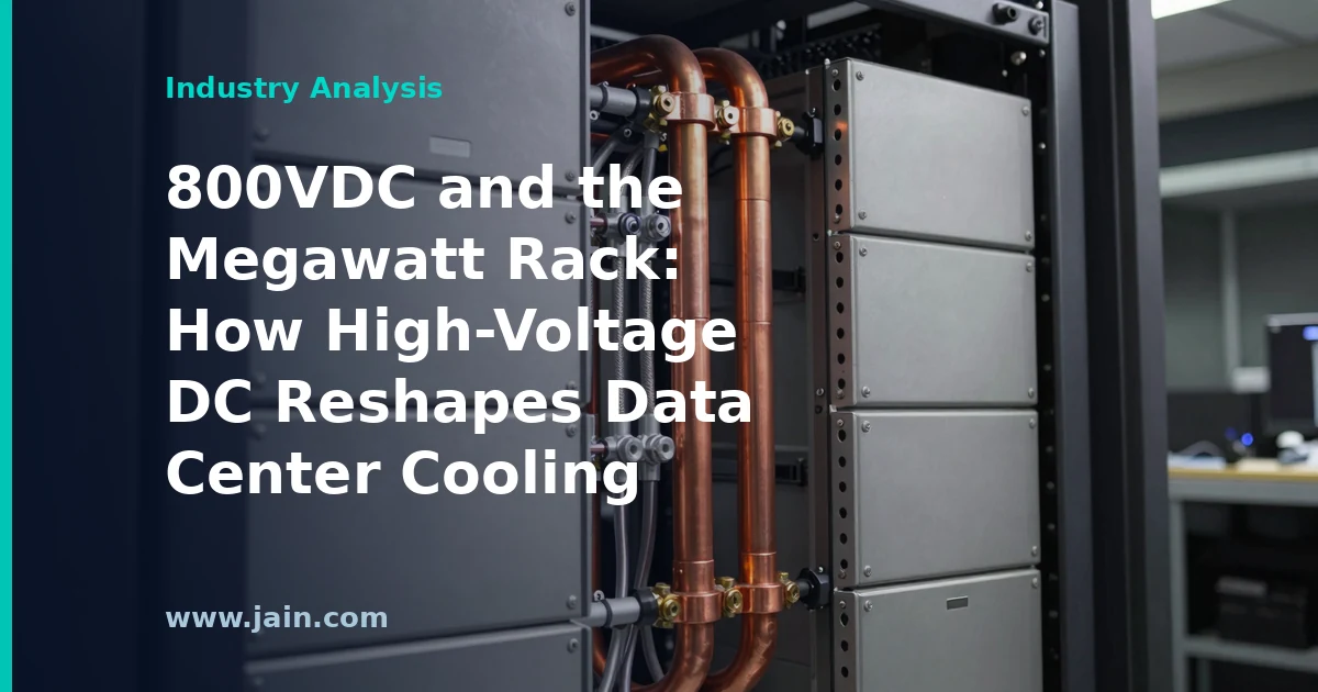
Data Center Dynamics has published an analysis of 800-volt direct current (800VDC) power distribution and its knock-on effects for data center cooling, examining the infrastructure evolution and operational impact of the architecture now being proposed for next-generation AI racks. The piece lands as the industry debates how facilities designed around alternating current (AC) and 54-volt in-rack distribution adapt to rack power densities approaching a megawatt.
Executive Summary
The subject is a plumbing-and-wiring story with strategic stakes: as AI accelerator racks climb toward megawatt-class power draws, the conventional approach — converting utility AC power through multiple stages down to low-voltage DC inside the rack — runs into hard physical limits on copper, conversion losses, and space. Moving distribution to 800VDC, an approach publicly championed by NVIDIA and partners across the power-electronics ecosystem for its next-generation rack designs, promises fewer conversion stages, dramatically thinner conductors, and higher end-to-end efficiency.
The DCD analysis focuses on the less-discussed second-order effect: what this does to cooling. Every watt saved in power conversion is a watt of heat that never has to be removed, but the racks 800VDC enables are so dense that liquid cooling becomes a prerequisite rather than an option. Power architecture and thermal architecture, historically designed by separate teams against separate budgets, are converging into a single engineering problem — and operators, colocation providers, and equipment vendors will all feel the shift.
Why a Power Story Is Really a Cooling Story
In a data center, electricity and heat are two views of the same quantity: essentially all power delivered to IT equipment leaves as heat that the cooling plant must reject. Every stage of power conversion — utility voltage to distribution voltage, AC to DC, high DC to the roughly one volt a chip core actually uses — wastes a slice of energy as heat, often inside the white space where cooling is most expensive. Collapsing conversion stages with 800VDC distribution reduces that parasitic load. But the same architecture exists to feed racks far denser than air can handle: at hundreds of kilowatts per rack and beyond, direct-to-chip liquid cooling with cold plates, coolant distribution units (CDUs), and facility water loops stops being an exotic option and becomes the baseline design.
That coupling changes how facilities get engineered. Busbar routing, cold-plate manifolds, leak detection, and serviceability now compete for the same rack volume. The DCD piece’s framing — implications, infrastructure evolution, operational impact — reflects a real shift in the industry conversation from “can we power it” to “can we power and cool it as one integrated system.”
What Actually Changes Between 54 Volts and 800
Today’s high-density AI racks typically distribute power internally at around 54 volts DC over copper busbars. Power scales with voltage times current, so at fixed voltage, a megawatt rack demands enormous current — and current is what sizes conductors, connectors, and their resistive losses. Raising distribution to 800VDC cuts the current for the same power by an order of magnitude, which is why the approach shrinks copper requirements and frees rack space for compute and cooling hardware. It also moves bulky AC-to-DC conversion equipment out of the rack into dedicated infrastructure, a further gift of space and a relocation of its heat.
For the thermal engineer, the ripple effects are concrete: less conversion loss inside the rack, but far more total heat per rack; new hot components (DC converters, solid-state protection devices) in new places; and coolant loops that must be designed around high-voltage conductors with appropriate creepage, isolation, and leak-response assumptions. None of this is unsolvable — electric vehicles and utility-scale solar have normalized high-voltage DC engineering — but it is genuinely new practice for most data center operations teams.
The Operational Bill: Skills, Safety, and Serviceability
The quiet cost of the transition is human. Data center technicians are trained on AC systems and low-voltage DC; 800VDC introduces different arc-flash behavior, different lockout and protection practices, and different failure modes, now interleaved with pressurized liquid-cooling loops in the same enclosure. Procedures for a coolant leak near an energized 800V busbar have to be written, trained, and drilled before the first rack lands. Vendors will point to sealed, engineered systems; operators will reasonably ask who is qualified to service them and on what schedule.
There is also a monitoring and commissioning dimension. When power and cooling are co-designed, so must be their telemetry: a CDU fault and a DC bus fault can each cascade into the other’s domain within seconds at megawatt densities. Operators evaluating 800VDC-era equipment should scrutinize integration of electrical and thermal controls as closely as the headline efficiency figures.
Winners, Losers, and the Retrofit Question
The clearest beneficiaries are power-electronics and liquid-cooling suppliers, which gain a generational replacement cycle, and hyperscale builders designing greenfield AI factories where the whole electrical-thermal stack can be specified at once. The harder position belongs to operators of existing facilities: buildings engineered around air cooling, AC distribution, and 10–30 kW racks cannot simply be re-declared 800VDC-ready. Some will retrofit power and cooling in tandem; others will find their most valuable asset is grid connection and land rather than the building itself.
For colocation providers and enterprise buyers, the pragmatic takeaway is sequencing. 800VDC is a roadmap item tied to next-generation rack platforms, not a description of most 2026 deployments — but cooling and electrical decisions made today have 15-to-20-year design lives. Facilities being planned now should at minimum preserve optionality: structural allowances for liquid loops, space for DC plant, and staff development that anticipates high-voltage practice.
Background
Data center power delivery has evolved in steps: from AC distribution to the server, to rack-level busbars at 12 and then 54 volts DC, each change driven by rising density. The AI buildout broke the curve — accelerator racks jumped from tens of kilowatts to hundreds, with roadmaps pointing toward a megawatt per cabinet, forcing the industry to revisit both how power reaches silicon and how heat leaves it. In 2025, NVIDIA and a wide ecosystem of power and cooling partners publicly outlined 800VDC distribution for next-generation rack platforms, borrowing high-voltage DC practice from electric vehicles and utility-scale solar.
Data Center Dynamics, the trade publication behind the source analysis, has tracked the parallel rise of liquid cooling from niche to necessity. The convergence of those two threads — high-voltage power and liquid thermal management as one co-designed system — is the backdrop for this piece and for facility design decisions now being made with multi-decade consequences.
Source: 800VDC data center cooling: Implications, infrastructure evolution and operational impact — Data Center Dynamics analysis of how 800-volt DC power architecture reshapes data center cooling design and operations, published April 24, 2026.