Tag: data center networking

  • Marvell’s $5.5B AI Optics Deal and the Interconnect Bottleneck

    Marvell’s $5.5B AI Optics Deal and the Interconnect Bottleneck

    A widely syndicated item from retail-investor research site simplywall.st, circulating through Google News, asks what Marvell Technology (Nasdaq: MRVL) gains from a $5.5 billion AI optics deal. Marvell is a US-based fabless chip designer whose largest end market is data center silicon, including the optical components that move data between AI servers.

    The syndicated text available to us consists of the headline and link only. It does not name a counterparty, state whether Marvell is the buyer or the seller, describe the consideration mix, or give a closing date. The $5.5 billion figure and the “AI optics” framing are the only substantive details carried in the source, and neither is accompanied in that material by a quote or a primary company disclosure.

    Executive Summary

    The headline points at a genuinely important shift, even though the source itself is thin. For most of the current AI build cycle, the constraint operators talked about was compute: how many accelerators could be bought, powered and cooled. Increasingly the binding constraint is the fabric between those accelerators. A training or inference cluster is only as fast as its slowest link, and the links are now measured in hundreds of thousands of optical connections per site.

    That is why a $5.5 billion transaction attached to “AI optics” is worth attention regardless of its direction. Optical interconnect sits at the intersection of two things that are hard to replicate: high-speed mixed-signal silicon, where Marvell has a strong franchise inherited from its Inphi acquisition, and photonics manufacturing, where supply has been tight through the AI cycle. A deal of this size in that space either consolidates a defensible position or monetises one.

    The honest caveat is that the material in front of us does not establish which. Readers evaluating the transaction should treat the $5.5 billion number as reported by a third-party analysis site and verify structure, counterparty and timing against Marvell’s own filings before drawing conclusions about accretion, market share or roadmap.

    Why the Wires Became the Bottleneck

    Modern AI clusters are not single computers. They are thousands of accelerators stitched together so tightly that software treats them as one machine. Two networks do that stitching. Scale-up connects a handful to a few dozen chips inside a rack at extremely high bandwidth and very low latency. Scale-out connects racks to each other across the hall. Both have had to grow roughly in step with accelerator performance, and accelerator performance has been growing faster than copper cabling can comfortably follow.

    Beyond a metre or two at current data rates, copper runs out of headroom and the signal degrades. That pushes traffic onto optics: lasers, fibre and the transceiver modules that convert electrical signals to light and back. Inside those modules sit digital signal processors, or DSPs, which clean up a distorted waveform so the receiving end can read it. Each generational jump, 400G to 800G to 1.6T per port, roughly doubles the data a single link carries and forces a redesign of that signal chain. Marvell’s electro-optics business, built largely on its 2021 Inphi acquisition, is one of the small number of places that silicon comes from.

    The economic consequence is that optics have moved from a rounding error to a meaningful share of cluster capital cost, and from a background concern to a live operational one. Optical modules consume power and they fail; at hundreds of thousands of links per site, even a low failure rate becomes a staffing and spares problem. Any vendor that can cut watts per bit or improve link reliability is selling something operators will pay for.

    What a $5.5 Billion Number Implies, in Either Direction

    Read as an acquisition, $5.5 billion is large but not transformative for a company of Marvell’s scale. It would signal that management sees interconnect as the durable part of the AI stack, and the questions that follow are conventional: what revenue and gross margin come with the assets, whether the consideration is cash, stock or both, how it affects the balance sheet, and how long integration takes relative to the eighteen-to-twenty-four-month cadence at which optical generations turn over. In fast-moving silicon markets, an acquired roadmap can age before it closes.

    Read as a divestiture, the same number tells a different story: capital recycled out of a components business and toward custom accelerator silicon, where Marvell designs bespoke chips for individual hyperscale customers. That path trades a broad merchant franchise for deeper exposure to a small number of very large buyers. Neither reading is inherently better. They imply different risk profiles, and the source material does not let us choose between them.

    What holds in both cases is that the buyers are concentrated. A handful of hyperscalers and large AI labs account for the bulk of demand for high-speed optics. Concentration is pleasant on the way up, because a single design win can move a quarter, and unpleasant on the way down, because a single deferred build can do the same. Any assessment of this transaction that ignores customer concentration is incomplete.

    Custom Silicon Plus Photonics: A Real Moat With Real Erosion Risk

    The strategic case for combining custom accelerator design with optical interconnect is coherent. A vendor that designs a customer’s chip and also supplies the links between those chips can co-optimise the two, and it becomes harder to displace because switching costs compound across the design cycle. That is a genuine moat, not a slogan.

    It is also under pressure from several directions at once, and an even-handed analysis has to say so. Broadcom competes across switching silicon, optical DSPs and custom accelerators simultaneously. Nvidia has strong incentives to keep its scale-up fabric proprietary and in-house. Specialists such as Credo and Astera Labs attack adjacent slices of the connectivity problem, and module manufacturers in the United States and Asia compete hard on cost. Meanwhile hyperscalers keep expanding their own silicon teams, which makes today’s supplier a candidate for tomorrow’s insourcing.

    The most interesting technical risk is co-packaged optics, or CPO, which moves the optical engine onto the same package as the switch or accelerator instead of into a pluggable module at the faceplate. Done well, CPO saves power and board area. It also changes which components carry value and could reduce the role of the standalone DSP that anchors part of Marvell’s franchise. CPO has been arriving more slowly than its advocates predicted, partly because pluggable modules are serviceable and CPO largely is not, but the direction of travel is worth watching. A $5.5 billion commitment in optics is a bet on how that transition resolves.

    Reading a Headline-Only Story Responsibly

    This is a case where the analysis is more substantiated than the news. The industry context is well established: interconnect is a real bottleneck, optics is a real chokepoint, and consolidation there is a rational strategy. The specific transaction, as carried in this source, is a dollar figure in a headline from a third-party research site.

    That is not a criticism of the publisher, whose format is short-form investor commentary rather than primary reporting. It is a caution about how such items propagate. A number repeated across aggregators acquires an authority its original sourcing may not support, and AI summarisation tends to accelerate that effect. The appropriate response is to anchor on primary documents: a company press release, an SEC filing, or a counterparty confirmation.

    For practitioners, the practical takeaway is independent of the deal’s details. If you are procuring capacity or designing clusters, interconnect supply, roadmap alignment and vendor concentration deserve the same diligence you already apply to accelerators and power. Consolidation among optics suppliers, whichever way this transaction runs, narrows the field you are negotiating with.

    Background

    Marvell Technology is a fabless semiconductor company, meaning it designs chips and outsources their manufacture to foundries. Founded in 1995 and headquartered in Santa Clara, California, it spent its early years in storage controllers and consumer connectivity before reorienting around infrastructure silicon under chief executive Matt Murphy. A sequence of acquisitions built that position: Cavium in networking processors, Aquantia in Ethernet, Innovium in switching, and Inphi in high-speed electro-optics, its largest deal to date.

    The data center is now Marvell’s principal end market, spanning custom accelerator silicon for hyperscale customers, Ethernet switching, storage controllers and the optical components that connect servers. The company has also been pruning: in 2025 it agreed to sell its automotive Ethernet business to Infineon, a move consistent with concentrating capital on AI infrastructure. That context is why a multibillion-dollar transaction in AI optics reads as strategy rather than opportunism, whichever side of it Marvell turns out to be on.

    Source: What Does Marvell Technology (MRVL) Gain From Its $5.5 Billion AI Optics Deal? — a short-form investor analysis item from simplywall.st, distributed via Google News, whose syndicated text carries the $5.5 billion figure without accompanying transaction details.

  • Astera Labs Surge Signals AI’s Interconnect Bottleneck

    Astera Labs Surge Signals AI’s Interconnect Bottleneck

    Astera Labs (Nasdaq: ALAB), a Santa Clara-based supplier of connectivity silicon for AI data centers, has reported record revenue from its AI connectivity chips, with its shares reported to have risen 116%, according to a Startup Fortune headline distributed through Google News. The company sells the components that move data between processors, memory and networks inside AI server racks.

    The source item consists of a headline and a link only, with no accompanying body text. It does not state the reporting period for the revenue record, the size of that revenue, or the window over which the 116% share move was measured. Those limits are worth stating up front, because they determine how much weight the number can carry.

    Executive Summary

    The headline claim is simple: record AI connectivity chip revenue at Astera Labs, and a 116% move in the stock. The significance is not the percentage. It is the category. Astera Labs does not make graphics processing units (GPUs), the accelerators that perform AI training and inference calculations. It makes the plumbing that connects them, and demand for plumbing is now growing fast enough to produce record quarters at a company that had no public market history before 2024.

    That matters because it marks a shift in where AI data center scarcity sits. For three years the binding constraint was accelerator supply. As accelerator counts per cluster rise into the tens of thousands, the harder engineering problem increasingly becomes keeping those chips fed with data: signal integrity across longer copper runs, memory bandwidth, and switching capacity between racks. Every one of those problems is an interconnect problem, and interconnect is a separate silicon supply chain from the GPU itself.

    For infrastructure buyers, the practical reading is that connectivity components are moving from a line item to a design constraint. For investors, the caution is that a single uncontextualised percentage from a headline-only source is a weak basis for conclusions about a company’s durable position in that supply chain.

    The Bottleneck Has Moved Down the Rack

    An AI training cluster is only as fast as its slowest shared resource. When a model is split across thousands of accelerators, those chips must exchange intermediate results constantly. If the links between them stall, expensive silicon sits idle. This is why the industry increasingly distinguishes between scale-up connectivity, meaning the very high bandwidth links inside a single server or rack, and scale-out connectivity, meaning the Ethernet or InfiniBand network joining racks together.

    Astera Labs’ product lines map onto exactly this problem. Its Aries retimers clean up and retransmit PCIe signals that would otherwise degrade over distance, PCIe being the standard bus that connects processors to accelerators and storage. Its Taurus modules do a comparable job for Ethernet cabling, its Leo controllers address Compute Express Link (CXL), a standard for pooling and sharing memory across devices, and its Scorpio switches route traffic within the fabric. In plain terms: the company sells the parts that stop a rack full of accelerators from becoming a traffic jam.

    The economic consequence is that connectivity content per rack rises faster than rack count. Denser accelerator packing means more links, longer effective signal paths, and more places where a signal needs regenerating. That is a structurally favourable position, and it is the strongest argument behind the headline. It is also an argument about the category, not proof about any one supplier’s share of it.

    What the Headline Substantiates, and What It Does Not

    The source establishes two things: that Astera Labs reported record AI connectivity chip revenue, and that a 116% share move was reported. It establishes almost nothing else. A 116% gain in a single session at a company of this size would be extraordinary and would ordinarily be framed as such; the same figure over a year, or since a prior low, or as a revenue growth rate, would carry very different meaning. The source does not say which, and a careful reader should not assume the most dramatic reading.

    Similarly, “record revenue” is a low bar for a company that listed on Nasdaq in March 2024 and has grown from a small base through the steepest part of the AI capital expenditure cycle. Records are the expected outcome of that trajectory, not evidence of a step change. The material questions, none of which the source answers, are gross margin trend, revenue concentration among a handful of hyperscale customers, and whether growth is coming from new design wins or from higher volumes on existing ones.

    None of this is a criticism of the company, which has not made the claim in this form. It is a criticism of a headline-only artefact being treated as a data point. The appropriate response is to treat the directional signal as credible and the magnitude as unverified pending the primary filing.

    Who Gains, and Who Is Exposed

    The clearest beneficiaries of an interconnect-led cycle are the merchant silicon suppliers with standards-track products: Astera Labs among them, alongside considerably larger competitors including Broadcom and Marvell, which sell switching, physical-layer and custom silicon into the same racks. Optical module makers and cable assembly suppliers benefit from the same trend. So, indirectly, do data center operators who have invested in the power and cooling density that high-bandwidth racks require, since interconnect gains are only realisable in facilities that can host the racks in the first place.

    The exposure runs in two directions. First, customer concentration: purchasing of this class of component is dominated by a small number of hyperscalers and AI labs, any one of which can shift a roadmap and materially change a supplier’s outlook. Second, standards risk. Interconnect is a consortium business, governed by PCIe, CXL, Ethernet and newer accelerator-fabric efforts such as UALink, plus proprietary alternatives from the largest accelerator vendors. A supplier’s position depends on which fabric the market adopts, and adoption is decided by buyers with the scale to build their own alternatives.

    For enterprise buyers, the practical implication is procurement discipline rather than urgency. Interconnect specifications now deserve the same scrutiny in an AI cluster tender as accelerator counts, particularly around which standards a design commits to and how much of the fabric is single-sourced.

    Background

    Astera Labs was founded in 2017 to address a problem that was then niche and is now central: as data rates climb, electrical signals inside servers degrade over distance, limiting how far apart components can sit and how densely a rack can be packed. The company built products around open standards, chiefly PCI Express, Compute Express Link and Ethernet, positioning itself as a merchant supplier to system builders rather than as a competitor to accelerator vendors. It listed on Nasdaq in March 2024.

    The wider market context is a multi-year surge in AI data center construction, in which the scarce resources have rotated over time: first accelerators, then power and grid connections, then cooling capacity for denser racks. Interconnect is the current addition to that list. Because it is governed largely by industry consortia, competitive position depends on both engineering execution and which standards the largest buyers ultimately choose to build around.

    Source: Astera Labs Stock Soars 116% on Record AI Connectivity Chip Revenue — a Startup Fortune headline distributed via Google News, published without accompanying body text or disclosed figures.

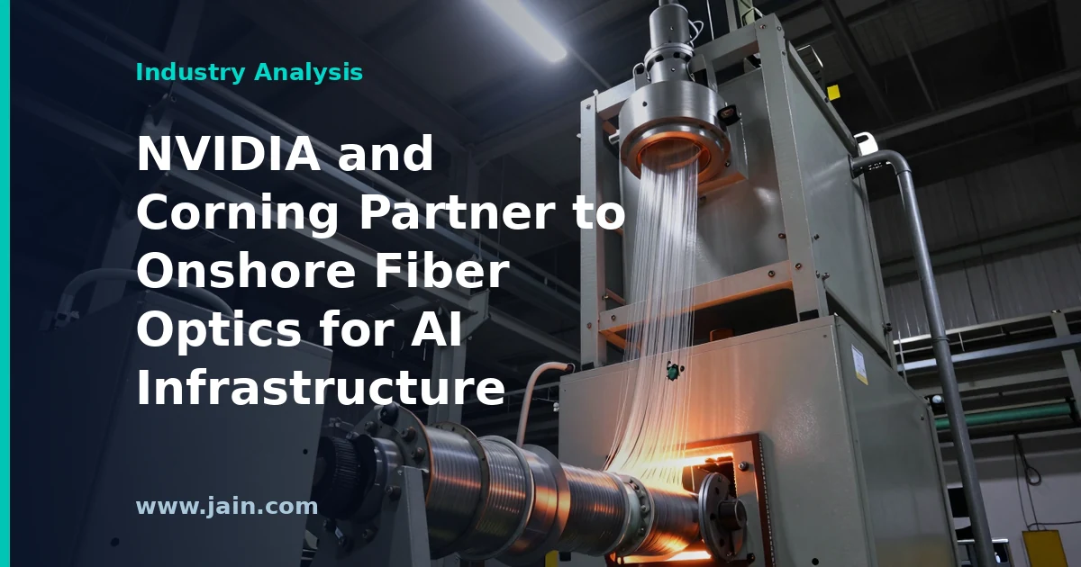
  • NVIDIA and Corning Partner to Onshore Fiber Optics for AI Infrastructure

    NVIDIA and Corning Partner to Onshore Fiber Optics for AI Infrastructure

    NVIDIA and Corning announced a long-term partnership on May 5, 2026, aimed at strengthening US manufacturing for AI infrastructure, according to a release published through the NVIDIA Newsroom. The tie-up pairs the dominant supplier of AI accelerator chips with the company that invented low-loss optical fiber and remains America’s leading producer of it.

    The announcement, as distributed, is headline-level: it frames the partnership around domestic manufacturing capacity for the optical components AI data centers consume, but the source text does not disclose financial terms, volumes, or specific facilities.

    Executive Summary

    The partnership signals something the AI build-out has made increasingly clear: the constraint on giant GPU clusters is no longer just chips. Modern AI data centers are, in a real sense, optical networks with computers attached — tens of thousands of processors stitched together by fiber links, each rack consuming far more optical connectivity than a traditional cloud facility. A chipmaker locking arms with a glass and fiber manufacturer is a recognition that the network fabric is now part of the product.

    For Corning, a long-term relationship with the largest buyer-influencer in AI infrastructure offers the kind of demand visibility that justifies factory investment. For NVIDIA, it extends a broader pattern of shoring up US-based supply for the components its platforms depend on. For everyone else — data center operators, competing optics suppliers, and policymakers pushing domestic manufacturing — the deal is a marker of where the AI supply chain is consolidating.

    What it is not, at least based on what the release makes public, is a quantified commitment. Without disclosed dollars, volumes, or timelines, the announcement is directionally significant but not yet measurable.

    Why AI Data Centers Are Suddenly a Fiber Story

    Training and running large AI models requires connecting thousands of GPUs so tightly that they behave like one machine. Every one of those connections — between chips, between servers, between rows of racks — increasingly runs over optical links, because light through glass fiber carries far more data over distance than copper wire can. The result is that an AI facility consumes multiples of the fiber, optical transceivers, and cable assemblies of a conventional data center of the same size.

    That is why an announcement between a semiconductor company and a materials manufacturer makes strategic sense. NVIDIA sells not just chips but entire cluster architectures, and those architectures are only as deliverable as their weakest supply line. Optical connectivity has repeatedly been a pinch point during the AI build-out, and securing it upstream is cheaper than discovering a shortage downstream.

    Onshoring the Optical Supply Chain

    The release’s framing — “strengthen US manufacturing” — places the deal squarely in the broader push to bring strategic component production back to American soil. Optical fiber and cable production is a global industry, and US policymakers have treated domestic capacity for critical infrastructure inputs as a national priority. A long-term partnership with an anchor customer is the classic mechanism for making onshoring economics work: manufacturers hesitate to build domestic capacity without demand certainty, and buyers hesitate to depend on capacity that does not yet exist. Pairing off resolves both hesitations at once.

    The trade-offs are real, though. Domestic manufacturing can carry higher costs than established overseas supply chains, and new capacity takes time to ramp. Whether this partnership changes the market depends on execution details the announcement does not provide — how much capacity, where, and by when.

    What It Means for Corning and the Competitive Field

    Corning brings unusual credibility to this role: it invented low-loss optical fiber in 1970 and has manufactured it in the United States for decades. A durable relationship with the central player in AI infrastructure gives it a privileged position in the fastest-growing segment of the optical market, and demand visibility that can underwrite capital spending shareholders might otherwise question.

    For competing fiber and optical component makers, the signal is more mixed. When anchor customers and suppliers pair off, remaining demand becomes more contestable but also more volatile. And for data center operators and enterprises buying connectivity, the second-order effect is worth watching: supply assurance for NVIDIA-aligned deployments could tighten availability elsewhere if overall capacity does not grow as fast as the partnership implies.

    Reading the Announcement Critically

    Corporate partnership announcements span a wide spectrum — from binding, take-or-pay purchase agreements to memoranda of understanding with no enforceable commitments. The source material here, distributed as a headline through a news aggregator, does not establish where on that spectrum this deal sits. No dollar figures, product mix, facility plans, or hiring numbers are cited in what was published.

    That does not make the announcement empty; both companies have reputations and existing US manufacturing footprints that lend it weight. But readers should treat the strategic direction as substantiated and the scale as unproven until either company attaches numbers — in capital expenditure disclosures, earnings commentary, or facility announcements — that can be verified against it.

    Background

    Corning, founded in 1851, is one of America’s oldest materials-science companies; its researchers invented low-loss optical fiber in 1970, the breakthrough that made modern telecommunications and the internet physically possible. It remains the leading US manufacturer of optical fiber, cable, and connectivity solutions for telecom carriers and data centers. NVIDIA, whose graphics processors became the workhorses of the AI boom, has grown into the central supplier of AI computing platforms and has increasingly emphasized building out US-based manufacturing for the infrastructure surrounding its chips.

    The partnership lands amid a historic wave of AI data center construction, in which optical networking — once a background utility — has become a recognized bottleneck, and amid a sustained US policy push to onshore manufacturing of strategically critical technology components.

    Source: NVIDIA and Corning Announce Long-Term Partnership to Strengthen US Manufacturing for AI Infrastructure — NVIDIA Newsroom release, May 5, 2026, announcing a long-term US manufacturing partnership for AI infrastructure optics.