
Tag: AI Accelerators

  • Google’s $12.2B Marvell Deal Reshapes the Custom AI Chip Race

    Google’s $12.2B Marvell Deal Reshapes the Custom AI Chip Race

    Google has expanded its custom AI chip partnership with Marvell Technology in a deal reported at $12.2 billion, according to multiple Yahoo Finance reports published this week. Broadcom — long regarded as Google’s incumbent partner for custom AI accelerators — saw its shares fall 6.2% on the news, while analyst fair-value estimates for Marvell edged higher.

    Executive Summary

    The reported agreement deepens Google’s relationship with Marvell for custom silicon — chips designed to a single customer’s specification rather than sold off the shelf. In AI infrastructure, these custom accelerators (often called XPUs or ASICs) are the hyperscalers’ primary lever for reducing dependence on Nvidia’s general-purpose GPUs, and the design partner that wins the engagement captures years of high-visibility revenue.

    The market reaction tells the story in one frame: Broadcom, which has been widely credited as the co-design partner behind Google’s Tensor Processing Units (TPUs), dropped 6.2%, while Marvell’s bull case strengthened. A $12.2 billion figure, if it represents committed or expected purchases, would be one of the larger custom-silicon engagements publicly reported — though the source articles leave the deal’s structure, duration, and scope largely undefined.

    For the broader AI infrastructure market, the significance is less about one stock move and more about confirmation of a trend: hyperscalers are dual-sourcing their chip design partners the same way they dual-source power, fiber, and data center capacity — to control cost, schedule risk, and negotiating leverage.

    Why Hyperscalers Refuse to Depend on One Chip Partner

    Custom AI accelerators are multi-year commitments. A hyperscaler like Google picks a design partner, co-develops a chip over 18–36 months, then ramps production across successive generations. That timeline creates lock-in — and lock-in creates pricing power for the partner. Broadcom’s custom-silicon business has been a major beneficiary of exactly that dynamic. By expanding work with Marvell, Google gains a credible second source, which pressures pricing on every future generation and insulates its TPU roadmap from any single vendor’s execution stumbles.

    This mirrors how large infrastructure buyers behave everywhere in the stack. No serious operator single-sources grid power, network transit, or construction contractors for a multi-gigawatt buildout. As custom silicon becomes as strategically important as the data centers that house it, the same procurement discipline is arriving in chip design.

    Broadcom’s 6.2% Drop: Signal Versus Substance

    A one-day 6.2% decline reflects what investors fear, not necessarily what Google has decided. The reports do not state that Google is reducing its Broadcom engagement — only that it is expanding Marvell’s. Those are different things: Google’s total accelerator demand is growing fast enough that two partners could both see rising volumes. The bearish reading is about share and leverage, not necessarily absolute revenue.

    That said, the concern is not irrational. In custom silicon, the design win for generation N strongly influences who builds generation N+1. If Marvell’s expanded role includes compute (the accelerator itself) rather than adjacent components such as networking or interconnect silicon, the competitive implications for the incumbent are materially larger. The source reporting does not settle that question — and it is the single most important unknown in this story.

    What $12.2 Billion Does — and Doesn’t — Tell Us

    Headline deal values in semiconductors deserve careful reading. A $12.2 billion figure could represent firm purchase commitments, a cumulative multi-year revenue expectation, or an analyst’s sizing of the opportunity — each with very different levels of certainty. The reports cited here frame it as changing Marvell’s bull case, which suggests investors are treating it as durable pipeline, but the articles do not disclose contract structure, timeline, or margin profile.

    Custom silicon also carries structurally lower gross margins than merchant chips, because the customer funds the design and captures much of the value. Marvell’s win is real in revenue-visibility terms; whether it is equally attractive in profitability terms depends on details not yet public.

    Downstream Effects on AI Infrastructure Buyers

    For enterprises and operators who buy cloud AI capacity rather than chips, this competition is quietly good news. Every credible alternative to Nvidia GPUs — and every second source within the custom-silicon supply chain — adds capacity to a market that has been supply-constrained for years. More TPU supply at better economics ultimately shows up as more available accelerated compute, and potentially better pricing, for Google Cloud customers. It also intensifies demand on the physical layer: more accelerator volume means more high-density data center space, more power procurement, and more advanced cooling — the parts of the stack where constraints now bind hardest.

    Background

    Google has designed its own AI accelerators — the TPU line — for roughly a decade, working with external semiconductor partners on design and production. Broadcom has long been identified in industry reporting as the principal partner behind that program, and custom accelerators for hyperscalers have become one of the fastest-growing segments in semiconductors as cloud providers seek alternatives to merchant GPUs. Marvell, meanwhile, has built its own custom-compute franchise serving hyperscale customers, making it the most frequently cited challenger to Broadcom in this market.

    The reported $12.2 billion expansion lands in that context: a two-horse race for hyperscaler design partnerships, where each win shapes multiple future chip generations and, downstream, the data center, power, and cooling infrastructure required to deploy them.

    Source: Broadcom (AVGO) Is Down 6.2% After Google Expands AI Chip Ties With Marvell — Yahoo Finance, with related Yahoo Finance coverage of Marvell’s reported $12.2 billion Google partnership expansion and its impact on analyst fair-value estimates.

  • AMD Says Instinct MI355X Sets a New Bar for DeepSeek Inference

    AMD Says Instinct MI355X Sets a New Bar for DeepSeek Inference

    AMD announced on June 11, 2026 that its Instinct MI355X accelerator has set a new performance bar for inference on DeepSeek models — the open-weight large language models from the Chinese AI lab whose efficiency-focused releases reshaped expectations for serving costs. Inference is the work of running a trained model to answer real requests, as opposed to training it in the first place.

    The claim, published by AMD itself, positions the MI355X — the flagship of AMD’s MI350 series — as a leading choice for the inference-heavy workloads that increasingly dominate AI infrastructure spending.

    Executive Summary

    AMD’s announcement is a benchmark claim, not a product launch: the company says the MI355X, its current flagship data-center GPU, delivers record-setting throughput when serving DeepSeek models. Because DeepSeek’s open-weight models are among the most widely deployed for self-hosted inference, they have become a de facto proving ground for accelerator vendors — a benchmark customers can actually reproduce, unlike proprietary-model results.

    The timing matters. The AI hardware market is shifting from a training-dominated buildout, where Nvidia’s ecosystem advantage is strongest, toward an inference era where cost per token served — the price of generating each unit of model output — is the metric that decides purchase orders. AMD’s pitch has consistently been large memory capacity and better price-performance for exactly this phase.

    What the headline claim does not establish, at least in the material visible here, is the specific numbers, the comparison baseline, or independent verification. Vendor benchmarks are a legitimate signal, but buyers should treat them as the opening of a conversation rather than its conclusion.

    Why DeepSeek Became the Benchmark That Matters

    DeepSeek’s models occupy an unusual position in the AI market: they are open-weight, meaning anyone can download and run them on their own hardware, and they were engineered from the start for inference efficiency. That combination made them the workload of choice for enterprises and cloud providers that want frontier-class capability without paying per-token API fees to a model vendor. When a chipmaker claims leadership on DeepSeek inference, it is claiming leadership on one of the workloads real customers actually deploy — which gives the claim more commercial weight than a synthetic benchmark, and also makes it more checkable, since third parties can rerun it.

    There is a second, subtler point: DeepSeek’s mixture-of-experts architecture — where only a fraction of the model’s parameters activate per request — stresses memory capacity and memory bandwidth more than raw compute. That plays to the MI355X’s most widely cited hardware advantage, its large high-bandwidth memory pool (288 GB of HBM3E per GPU, per AMD’s published specifications for the MI350 series). Fitting a large model on fewer GPUs reduces the interconnect traffic and server count needed to serve it, which is where inference economics are won or lost.

    The Inference Era Rewrites the Competitive Math

    Training a frontier model is a rare, massive event; serving it to millions of users is a continuous, compounding cost. As deployed AI applications scale, industry spending is tilting toward inference, and that shift changes what buyers optimize for. In training, ecosystem maturity and cluster-scale networking — Nvidia’s strongholds — dominate the decision. In inference, the calculus is simpler and more mercenary: tokens per second, per dollar, per watt. Every point of throughput a rival accelerator gains translates directly into rack space, power, and capital that an operator does not have to buy.

    This is why AMD keeps aiming its benchmark artillery at inference rather than training. It is the segment where switching costs are lowest — an inference deployment of an open-weight model is far easier to port between hardware vendors than a training pipeline — and where AMD’s ROCm software stack, historically its weakest flank against Nvidia’s CUDA, faces the least demanding compatibility burden. For data-center operators, a credible second source of inference silicon is leverage in every negotiation, whichever vendor ultimately wins the deal.

    A Vendor Benchmark Is a Claim, Not a Verdict

    The announcement comes from AMD’s own newsroom, and the standard cautions apply — as they would to any vendor, including Nvidia, whose competitive benchmarks deserve identical scrutiny. Benchmark results are exquisitely sensitive to configuration: batch size, input and output sequence lengths, quantization (running the model at reduced numerical precision to go faster), and which competing hardware and software versions form the baseline. A ‘new bar’ can be genuine engineering progress, a favorable test setup, or both at once. The release headline, on its own, does not let a reader distinguish these cases.

    The constructive reading is that publishing reproducible claims on an open-weight model invites exactly the third-party validation that settles such questions. If independent labs and cloud customers can replicate the numbers on production-shaped workloads, the claim hardens into a real competitive fact. If the result holds only under narrow conditions, the market will find that out quickly too — one of the healthier dynamics the open-weight ecosystem has introduced to hardware marketing.

    Background

    AMD has spent a decade rebuilding itself into the principal challenger to Nvidia in data-center silicon, first in CPUs with EPYC and more recently in AI accelerators with the Instinct line. The MI300 series, launched in late 2023, gave AMD its first broadly adopted AI GPU; the MI350 series that followed in 2025, including the MI355X, extended its strategy of packing more high-bandwidth memory per chip than competing parts to win inference workloads.

    DeepSeek entered the global spotlight in early 2025 when its efficient open-weight models demonstrated that frontier-class AI could be trained and served at far lower cost than prevailing assumptions, briefly shaking AI-infrastructure markets. Since then its models have become a standard workload for measuring inference performance — turning each new hardware generation’s ‘DeepSeek numbers’ into a competitive scoreboard watched by chipmakers, cloud providers, and investors alike.

    Source: AMD Instinct MI355X GPU Sets a New Bar for DeepSeek Inference — AMD, the company’s announcement of record DeepSeek inference performance on its flagship accelerator.

  • d-Matrix Corsair Hits Full Production: A Challenger to the AI Inference Status Quo

    d-Matrix Corsair Hits Full Production: A Challenger to the AI Inference Status Quo

    Silicon Valley chip startup d-Matrix announced on June 10, 2026 that Corsair, its flagship AI inference accelerator, has entered full production, with the company attributing the ramp to customer demand. Corsair is a PCIe-card accelerator built on d-Matrix’s digital in-memory compute architecture, designed to run large language model inference — the work of generating answers from already-trained models — faster and more efficiently than general-purpose GPUs.

    Executive Summary

    d-Matrix says its Corsair inference platform has moved from early availability into full production. For a fabless semiconductor startup, that transition is one of the hardest milestones in the business: it signals that the design, manufacturing partners, packaging, and software stack are mature enough to ship at volume rather than in evaluation quantities. The company frames the ramp as demand-driven, though the release does not disclose shipment volumes, named customers, or revenue.

    The announcement matters because it lands in the middle of the industry’s most consequential architectural debate: whether AI inference — now widely expected to dwarf training as a share of total AI compute spending — will remain a GPU market, or fracture into specialized silicon. Corsair is a purpose-built bet that inference is fundamentally a memory problem, not a compute problem, and that an architecture which collapses the distance between memory and math can win on cost and energy per token. Full production is the point at which that thesis stops being a slide deck and starts being testable in customer data centers.

    The Memory-Bandwidth Wall, Explained

    When a large language model generates text, the dominant cost is not arithmetic — it is moving the model’s billions of parameters from memory to the processor over and over, once per generated token. Processors have gotten faster far more quickly than memory has gotten closer, a gap the industry calls the memory-bandwidth wall. GPUs attack it with expensive stacks of high-bandwidth memory (HBM) bolted alongside the compute die; d-Matrix attacks it by performing the math inside the memory arrays themselves, an approach called digital in-memory compute. Less data movement means, in principle, lower latency and less energy per token.

    The architectural logic is sound and the problem is real — memory bandwidth, not raw FLOPS, is the binding constraint on most production LLM serving today. The open question has never been whether in-memory compute is elegant, but whether it can be manufactured at scale, programmed easily, and priced competitively. A full-production milestone speaks directly to the first of those three tests.

    From Demo Silicon to Volume: Why This Milestone Is the Hard One

    The graveyard of AI chip startups is full of companies that produced impressive demonstration silicon but never crossed into volume manufacturing. Getting there requires acceptable yields from foundry partners, stable supply of advanced packaging, qualified server integrations, and a software stack that customers other than the vendor’s own engineers can actually use. By declaring full production, d-Matrix is asserting it has cleared those gates.

    What the release does not do is quantify the claim. “Full production to meet customer demand” is a statement about readiness, not about scale: no unit volumes, deployment sizes, or purchasers are disclosed. That is typical for a private company’s press release, but it means the milestone should be read as necessary rather than sufficient evidence of commercial traction. The verifiable signals — named customers, independent benchmarks, follow-on orders — come later, and observers should watch for them.

    The Economics of Challenging an Incumbent

    Every inference challenger faces the same asymmetry: Nvidia’s advantage is only partly the silicon. Its CUDA software ecosystem, developer familiarity, and guaranteed supply relationships make GPUs the default even where specialized chips post better numbers on paper. Challengers such as Groq, Cerebras, and SambaNova — and the hyperscalers’ in-house chips like Google’s TPUs and Amazon’s Inferentia — have each carved positions by competing on cost per token, latency, or energy rather than generality.

    d-Matrix’s opening is real, though. Inference is a workload buyers purchase continuously, priced per token, which makes operating cost — dominated by power and hardware amortization — brutally legible. Enterprises and cloud providers are also actively seeking second sources to gain pricing leverage over the GPU supply chain. A challenger does not need to displace the incumbent to build a substantial business; it needs to win the subset of workloads where its architecture’s advantages are largest and the switching costs are manageable.

    What It Means for the Data Center

    For data-center operators, the interesting property of accelerators like Corsair is the form factor: PCIe cards that slot into standard servers, rather than the dense, increasingly liquid-cooled rack-scale systems that frontier GPUs demand. If inference-optimized silicon delivers competitive throughput at meaningfully lower power per token — a claim d-Matrix has consistently made in its marketing, and one that independent benchmarking will need to validate — it extends the useful life of conventional air-cooled facilities that cannot economically retrofit for 100-kilowatt racks.

    That has second-order implications for the industry’s power crunch. Inference demand is growing at exactly the moment grid interconnection has become the limiting factor on data-center construction. Any architecture that serves more tokens per megawatt is, in effect, a capacity play — and that, more than any single benchmark, is why purpose-built inference silicon keeps attracting capital.

    Background

    Founded in 2019, d-Matrix spent its first years developing digital in-memory compute through successive test chips before unveiling Corsair in late 2024 as its first volume product, aimed squarely at low-latency large language model serving. The company has raised several hundred million dollars from investors including Microsoft’s M12, Temasek, SK hynix, and Playground Global — one of the better-capitalized entrants in a crowded field of AI chip startups formed on the thesis that inference workloads will eventually dwarf training.

    That thesis has moved from contrarian to consensus: as deployed AI applications scale, the recurring cost of serving models has become the industry’s central economic problem, and the market for inference-optimized alternatives to GPUs has drawn challengers ranging from venture-backed startups to the hyperscalers’ own silicon programs. Full production of Corsair marks d-Matrix’s transition from architectural argument to shipping product in that contest.

    Source: d-Matrix Corsair AI Inference Platform Enters Full Production to Meet Customer Demand — company press release via PR Newswire, June 10, 2026, announcing the production ramp of d-Matrix’s inference accelerator platform.

  • Google TPU v8 vs Nvidia: Inference Is Redrawing the AI Compute Map

    Google TPU v8 vs Nvidia: Inference Is Redrawing the AI Compute Map

    On May 29, 2026, investment research firm IO Fund published an analysis arguing that Google’s eighth-generation Tensor Processing Unit (TPU v8) represents a meaningful challenge to Nvidia’s dominance of AI computing — and that the industry’s shift from training AI models to running them, known as inference, is rewriting who captures value in the AI market.

    The piece is analyst commentary rather than a company announcement: neither Google nor Nvidia issued the claims, and the material available does not include chip specifications, benchmarks, pricing, or customer commitments.

    Executive Summary

    The thesis at the center of the analysis is straightforward: the AI compute market that Nvidia came to dominate was built on training — the enormously expensive, one-time process of teaching a model. As AI products mature, spending shifts toward inference — the everyday work of answering queries, generating text and images, and serving applications to users. Inference runs continuously, at massive scale, and its economics reward cost-per-query and energy efficiency over raw peak performance.

    Google is the one hyperscaler that has designed its own AI accelerator across eight generations, and it both consumes TPUs internally and rents them to customers through Google Cloud. If inference becomes the dominant workload, the argument goes, a vertically integrated chip tuned for serving costs could take share that merchant GPUs currently hold by default.

    Why it matters: even a partial shift of inference workloads to non-Nvidia silicon would ripple through chip suppliers, cloud pricing, and the design of the data centers that house all of it. But readers should note what is being claimed versus what is being shown — the source material asserts the competitive framing without publishing head-to-head performance or cost data.

    From Training Arms Race to Inference Economics

    Training a frontier AI model is a capital project: a huge cluster runs for weeks or months, and buyers pay almost any price for the fastest available hardware. Inference is an operating expense: every chatbot reply, search summary, and generated image is a small compute job repeated billions of times. That changes the buying criteria. For training, time-to-result dominates; for inference, what matters is cost per token served, latency, and performance per watt — how much useful output a chip produces for each unit of electricity.

    This is why analysts increasingly frame inference as the market’s center of gravity. A workload that runs 24/7 in production is exquisitely sensitive to efficiency, and a chip that is modestly slower but meaningfully cheaper to operate can win business that a peak-performance chip cannot. The IO Fund headline captures that logic; what the available material does not provide is data quantifying how TPU v8 actually performs on those metrics against Nvidia’s current parts.

    Custom Silicon and the Limits of the CUDA Moat

    Nvidia’s advantage has never been hardware alone. CUDA, its programming platform, is the software layer nearly all AI development targets, and switching away from it carries real engineering cost. That moat is strongest where code is bespoke and experimental — which describes training research well. Inference is different: production models are increasingly served through standardized frameworks and compilers that can target multiple chip types, lowering the switching cost that protects the incumbent.

    Google’s structural position is also unusual. Unlike merchant chipmakers, Google does not need to win sockets in other companies’ data centers to justify TPU development — its own search, ads, and Gemini workloads provide guaranteed internal demand, and Google Cloud monetizes the surplus. Amazon and Microsoft have followed the same playbook with their own accelerators. The open question, which the source material does not answer, is whether any hyperscaler chip has yet attracted large third-party inference workloads at scale, or whether custom silicon remains mostly an internal cost-reduction tool.

    What Inference-First Compute Means for Physical Infrastructure

    The training-to-inference shift is not just a chip story; it reshapes data centers. Training concentrates compute in a few gigawatt-scale campuses. Inference pulls in the opposite direction: serving users at low latency favors capacity distributed closer to population centers, with high-bandwidth connectivity to move requests and responses rather than model weights. For data center operators and network providers, an inference-heavy market means demand for more sites, in more markets, with different power and cooling profiles than monolithic training clusters.

    Efficiency claims matter here too. Power availability is the binding constraint on data center growth in most major markets, so performance-per-watt improvements in accelerators translate directly into how much AI capacity a given substation can support. Any credible challenger to Nvidia will be judged as much on watts as on FLOPS — a reminder that the AI market’s referee is increasingly the electric grid.

    Reading the Claim Like a Buyer

    For enterprises and cloud customers, the practical takeaway is not to pick a winner but to price the competition. A credible TPU alternative — even one adopted mainly inside Google — pressures accelerator pricing and cloud inference rates across the board, because Nvidia’s largest customers gain negotiating leverage. Buyers evaluating platforms should ask vendors for workload-specific benchmarks (their models, their traffic patterns) rather than headline chip comparisons, and should weigh portability: an inference stack built on open frameworks preserves the option to chase better economics as this rivalry plays out.

    It is equally fair to stress-test the bear case on Nvidia. The company has repeatedly absorbed inference-era challenges by iterating its own inference-optimized products and software, and market-share shifts in semiconductors tend to be slower than analyst narratives suggest. A headline announcing that the market is being ‘rewritten’ is a thesis, not a measurement — and the same skepticism should apply to Google-favorable and Nvidia-favorable framings alike.

    Background

    Google disclosed its first Tensor Processing Unit in 2016, making it the earliest hyperscaler to design custom AI silicon rather than rely solely on merchant chips. Successive TPU generations scaled from internal inference workloads to full training clusters offered through Google Cloud, and the seventh generation, Ironwood, announced in April 2025, was explicitly positioned as an inference-first chip — a signal of where Google believed the market was heading.

    Nvidia, meanwhile, converted its graphics-processor franchise into overwhelming leadership of AI training hardware, propelled by the generative-AI buildout that began in late 2022 and reinforced by its CUDA software ecosystem. The tension between merchant GPUs and hyperscaler custom silicon — Amazon’s Trainium, Microsoft’s Maia, Google’s TPUs — has become one of the defining structural questions of the AI infrastructure market, and the training-versus-inference spending mix is the variable most likely to decide it.

    Source: Google TPU v8 vs Nvidia: How Inference Is Rewriting the AI Market — IO Fund analysis, published May 29, 2026, arguing that the shift from AI training to inference is reshaping competition between Google’s custom TPU silicon and Nvidia’s GPUs.

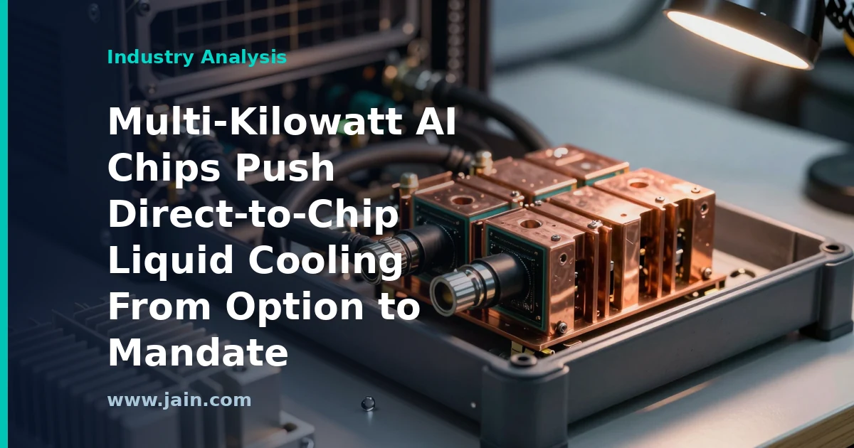
  • Multi-Kilowatt AI Chips Push Direct-to-Chip Liquid Cooling From Option to Mandate

    Multi-Kilowatt AI Chips Push Direct-to-Chip Liquid Cooling From Option to Mandate

    Engineering trade publication Electronics360 published an analysis on May 24, 2026 arguing that direct-to-chip (D2C) liquid cooling — circulating coolant through cold plates mounted directly on processors — has crossed from a design option to a practical requirement, driven by AI accelerator chips whose power draw has reached the multi-kilowatt range per device.

    The piece frames this as the end of an era: air cooling, the default thermal strategy for data centers since the industry’s beginning, can no longer keep pace with the heat that flagship AI silicon produces in the small area of a single chip package.

    Executive Summary

    The core claim is thermodynamic rather than commercial: individual AI processors now dissipate thousands of watts each, and moving that much heat out of a dense rack with air alone requires airflow volumes and temperature differentials that become impractical or impossible at the densities AI clusters demand. Direct-to-chip liquid cooling, which places a liquid-filled cold plate against the chip itself, removes heat far more efficiently because liquids carry heat orders of magnitude better than air.

    Why it matters: if D2C is genuinely mandatory rather than optional, every layer of the data-center stack changes — facility design, plumbing, power distribution, rack architecture, maintenance skills, and capital budgets. Operators of existing air-cooled facilities face retrofit decisions, and new builds are being designed liquid-first. For an industry that standardized on air handling for decades, this is a foundational transition, not an incremental upgrade.

    Physics Ended the Debate Before the Market Did

    Air cooling persisted as the default not because it was elegant but because it was cheap, simple, and universally understood. Its limitation is fundamental: air is a poor heat conductor, so cooling a hotter chip means moving more air, faster, across larger heatsinks. As AI accelerators pushed past one kilowatt per device — with roadmaps pointing well beyond — the heat concentrated in a few square centimeters of silicon began to exceed what any realistic airflow can absorb. Water and engineered coolants transfer heat dramatically more effectively, which is why cold plates bolted directly onto the chip package have become the pragmatic answer.

    The word ‘mandatory’ in the source’s framing is worth taking seriously but precisely. Air cooling is not disappearing from data centers generally — the vast installed base of conventional enterprise and cloud workloads runs at rack densities air handles fine. The mandate applies to the frontier: dense AI training and inference clusters built around multi-kilowatt accelerators. That distinction matters for anyone budgeting a transition.

    The Retrofit Question Splits the Market

    Liquid-first design is straightforward in a new build: coolant distribution units, manifolds, leak detection, and higher floor loading are engineered in from day one. Retrofitting an existing air-cooled facility is harder. Piping must be routed through spaces never designed for it, water supply and heat-rejection capacity must be added, and operations teams must learn to manage a system where a leak — rare but nonzero — sits inches from expensive silicon.

    This creates a divergence in asset value across the industry. Facilities that can economically accept liquid cooling — because of their power capacity, structure, and location — become more valuable as AI demand grows. Older facilities that cannot may be relegated to lower-density workloads. Colocation providers, hyperscalers, and enterprise operators are all making that assessment now, and the answers will shape which real estate wins the AI buildout.

    A New Supply Chain Rises Around the Cold Plate

    A shift of this scale redraws the vendor landscape. Demand moves toward cold plates, coolant distribution units, quick-disconnect fittings, dielectric and water-based coolants, leak-detection systems, and rear-door or facility-level heat exchangers — categories that were niche a few years ago. Established thermal-management and precision-cooling vendors are competing with newer specialists, and chip and server makers increasingly ship liquid-ready designs, effectively deciding the question for their customers.

    There is also an efficiency dividend. Because liquid captures heat at the source, less energy is spent on fans and air handling, and the warm coolant leaves at temperatures useful for heat reuse in some settings. For operators facing scrutiny over data-center energy consumption, D2C offers a genuine efficiency story — though it introduces its own considerations around water use and coolant handling that deserve equally honest accounting.

    Background

    For most of computing history, data centers were cooled the same way: chilled air pushed through raised floors or ducts, across finned metal heatsinks, and back to air-handling units. That model worked because individual chips drew tens or hundreds of watts. The AI era broke the assumption — training and running large models rewards packing the most powerful accelerators as densely as possible, and each generation of AI silicon has raised per-chip power substantially, crossing the kilowatt mark and continuing upward.

    Liquid cooling itself is not new; mainframes and supercomputers used water cooling decades ago before commodity air-cooled servers displaced them on cost. What has changed is that the physics that once made liquid cooling a supercomputing niche now applies to mainstream AI infrastructure, pulling a once-specialist discipline back to the center of data-center design.

    Source: Multi-kilowatt chips make D2C cooling mandatory — Electronics360 analysis (May 24, 2026) on why multi-kilowatt AI processors are forcing data centers from air cooling to direct-to-chip liquid cooling.