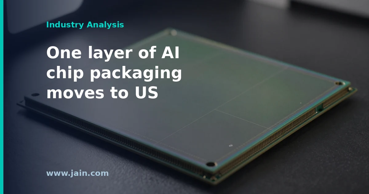
Two major chipmakers, GlobalFoundries and Taiwan Semiconductor Manufacturing Company, the world’s largest contract chipmaker, have struck a $2 billion deal to make a key chip part in the United States.
The part is a silicon “interposer”: a thin slab of silicon that sits under an artificial intelligence processor and wires it to its memory, like a shared floor both chips are mounted on. The packaging step built around it has been one of the main limits on how many artificial intelligence chips get shipped.
Making it in America could add supply outside Taiwan. But it covers one step, not the whole chip.
Yahoo Finance reported that GlobalFoundries and TSMC have reached a $2 billion deal for silicon interposers produced in the United States. Silicon interposers are the base layer in the advanced packages that join high-end AI processors to stacked high-bandwidth memory, which places the agreement inside the part of the GPU supply chain that has repeatedly constrained output.
The deal follows TSMC’s October 8 Form 6-K, its September 2026 revenue report, which showed consolidated revenue of roughly NT$511.86 billion for the month, up 54.6 percent from September 2025, and NT$3,898.73 billion for January through September, up 41.1 percent year over year.
Executive Summary
The headline facts are simple: a $2 billion agreement between the world’s largest contract chipmaker and a US-headquartered specialty foundry, covering a component that is made in the United States. The interposer is not a commodity part. It is a large piece of silicon, patterned in a wafer fab with fine wiring and vertical connections called through-silicon vias. AI accelerators mount their compute die and memory stacks on it side by side.
That matters because AI chip supply has been gated less by the ability to make processors than by the ability to package them with memory. Making interposers in the US adds a domestic source for one input to that packaging flow. However, an interposer is an intermediate part. Until the companies say where the rest of the package is assembled, the deal shows where part of the bottleneck can be relieved, not that it has been.
For GlobalFoundries, a $2 billion commitment tied to AI packaging is a significant new line for a foundry that stepped back from the leading-edge process race in 2018. For TSMC, whose September revenue alone was more than NT$500 billion, the deal is small in financial terms. Its importance is geographic and logistical.
Why the Interposer Sits on AI’s Critical Path
The most capable AI accelerators are not a single chip. They are assemblies. A large processor die sits next to several stacks of high-bandwidth memory (HBM), DRAM chips stacked vertically to deliver very fast data access. These parts have to talk to each other across thousands of extremely fine connections, far denser than an ordinary circuit board can carry. The silicon interposer solves this. It is a slab of silicon wired with lithography, the same patterning process used to make chips, so the processor and memory can be packed millimetres apart and connected at chip-level density.
TSMC’s version of this approach is CoWoS, short for chip-on-wafer-on-substrate. Dies are bonded onto an interposer wafer, which is then mounted on a conventional package substrate. In recent years, CoWoS capacity has been widely identified as a binding constraint on AI accelerator shipments. The processors could be fabricated, but there was not enough capacity to package them with their memory. Interposers are one input to that flow. Because they are made in a fab rather than an assembly house, adding interposer supply requires wafer capacity with the right tooling, not just more packaging lines.
What Onshoring One Layer Does, and What It Doesn’t
This is the substance behind the headline. A US-based interposer source moves one fab-made step of AI packaging onto American soil. That has real value. It adds a source outside Taiwan for a component tied to a known chokepoint. It suits a mature, non-leading-edge process, which plays to GlobalFoundries’ strengths in its New York and Vermont fabs. It also gives chip designers and their hyperscale customers, the largest cloud and AI operators, a domestic option to cite when they are asked about supply resilience.
But an interposer alone does not make a finished accelerator. After the interposer is made, the processor dies and memory stacks must be bonded onto it. The assembly must then be mounted on a substrate, tested, and shipped. If those steps remain in Taiwan, US-made interposers simply cross the Pacific in the opposite direction from the processors. Much of the processor output from TSMC’s Arizona fabs has itself needed to return to Taiwan for advanced packaging. The deal becomes a genuinely domestic AI supply chain only when it pairs with US assembly capacity. TSMC said in March 2025 that its expanded Arizona plans include advanced packaging facilities, and its October 6-K shows continued financial support for US subsidiaries, recording lending to TSMC Washington and guarantees for TSMC Arizona. Connecting the interposer supply to that assembly capacity is the step that would turn a single onshored layer into an onshored package.
The packaging variant also matters. TSMC’s family includes the original CoWoS-S, which uses a full silicon interposer, and newer variants such as CoWoS-L, which replace the full interposer with smaller embedded silicon bridges. If flagship accelerators continue shifting toward bridge-based designs, the market for full-size interposers looks different. Which products these US interposers serve will determine how much of the bottleneck they actually touch.
Reading $2 Billion Against Each Company’s Scale
For TSMC, the figure is modest. Its September revenue was about NT$511.86 billion, and its year-to-date revenue was NT$3,898.73 billion, up 41.1 percent. A $2 billion agreement is not a material financial event at that scale. It is a capacity and location decision. Choosing a domestic partner for a mature-process component frees TSMC to focus its own capital elsewhere while adding a US element to its packaging chain.
For GlobalFoundries, the calculus runs the other way. A foundry that chose in 2018 to stop pursuing the most advanced process nodes now has a direct line into the most supply-constrained segment of the AI hardware market, using processes it already runs. That makes it a significant win, though its annual revenue impact cannot be assessed until the contract’s duration and ramp are known. The two companies were once adversaries in a patent dispute that they settled in 2019 with a broad cross-license. A supply relationship on AI packaging is a notable evolution from that history.
Background
TSMC, founded in Taiwan in 1987, is the world’s largest contract chipmaker. It manufactures processors for most leading AI chip designers, and its CoWoS packaging has become central to AI accelerator supply. It is building fabs in Arizona and has said its US plans include advanced packaging. GlobalFoundries, spun out of AMD in 2009, runs fabs in Malta, New York; Essex Junction, Vermont; Dresden; and Singapore. It stopped pursuing the most advanced process nodes in 2018 to focus on specialty technologies.
The two companies settled a patent dispute in 2019 with a broad cross-license. Their new interposer agreement places GlobalFoundries’ US mature-process capacity inside the AI packaging flow that TSMC dominates.
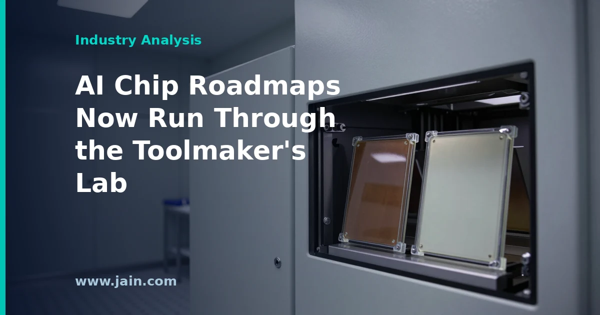
Intel, the American chipmaker, is expanding its research at a $5 billion lab in Silicon Valley run by Applied Materials, the company that builds the machines used to make computer chips.
The twist: Intel’s biggest rival in making chips for other companies, Taiwan Semiconductor Manufacturing Company, signed on to the same lab earlier this year. Two fierce competitors will be inventing future chips under one roof.
Why it matters: the chips behind artificial intelligence keep getting harder to make, and more of that early invention now happens at the machine maker, not inside any one chip company.
shattered.io reported that Applied Materials and Intel announced on October 6, 2026 an expanded collaboration on next-generation transistors, interconnects and advanced packaging, centered on Applied’s EPIC Center in Silicon Valley and Intel’s research campus in Hillsboro, Oregon. The work explicitly includes Foveros, Intel’s technology for stacking chip components vertically.
The EPIC Center, first pledged in May 2023 as an investment of up to $4 billion, is now described as a $5 billion facility. TSMC was confirmed as a founding partner in May 2026, five months before Intel’s expanded role was announced. No dollar figure, node target or performance goal was attached to the Intel agreement.
Executive Summary
Applied Materials, whose equipment sits inside virtually every leading-edge chip factory, now counts the two most closely watched advanced logic foundries (contract chip manufacturers) as research partners at the same facility. Intel’s expanded role covers the full stack of problems that limit AI processors: the transistors themselves, the microscopic wiring that connects them, and the packaging that joins multiple chip pieces into one product.
Intel CEO Lip-Bu Tan tied the work directly to AI demand, citing the need for gains in performance, power efficiency and packaging, and described Applied as an important partner in moving new technology from the lab into high-volume manufacturing in the United States. Intel Foundry’s chief technology and operations officer, Naga Chandrasekaran, framed faster R&D as critical to keeping pace with AI infrastructure buildout.
The significance lies less in any single deliverable, since none was disclosed, than in where the work is happening. When rival foundries both co-develop processes inside a toolmaker’s lab, the equipment vendor becomes a shared starting point for next-generation AI silicon.
Why the Toolmaker’s Lab Is Becoming the Starting Line
New chip generations do not begin at the factory. They begin with materials and process experiments: which film to deposit, how to etch a structure a few atoms wide, how to bond two pieces of silicon face to face. Those experiments depend on the equipment that will eventually run in production, which is why chipmakers co-develop processes with toolmakers. The EPIC Center, short for Equipment and Process Innovation and Commercialization, was built to formalize that step, with more than 180,000 square feet of cleanroom (ultra-clean manufacturing space) planned and up to 2,000 engineering jobs.
The scope of the Intel work maps onto the three constraints that matter most for AI processors. Front-end-of-line research targets the transistor layer. Back-end-of-line research targets interconnects, the wiring stacked above the transistors, where electrical resistance grows as features shrink and can become a bigger limit on speed and power than the transistors themselves. Packaging research, including Intel’s Foveros 3D stacking of chiplets (smaller dies combined into one package), targets interconnect density, power delivery and heat, all of which limit how much compute can be packed into an AI accelerator.
With TSMC as a founding partner and Intel as an expanded partner, at least part of the early-stage work on both companies’ next-generation AI silicon now passes through the same equipment vendor’s facility. That does not mean the two share designs or results; it means the toolmaker sees, and helps shape, both roadmaps. For AI chip designers who buy foundry capacity, it suggests that the process innovations available to them will increasingly be co-developed with Applied rather than invented in isolation inside one foundry.
Intel’s Math: A $2.1 Billion Loss and a Need for Outside Customers
Intel Foundry, the division that manufactures chips for Intel and outside customers, posted $5.8 billion in revenue and a $2.1 billion operating loss in its most recently reported quarter, a $348 million improvement on the prior period. Intel has raised its 2026 capital spending guidance to more than $20 billion company-wide, citing stronger customer-demand signals.
The division’s path to profitability runs through external customers, and winning them requires showing that Intel’s advanced nodes and packaging can match TSMC on schedule and yield. Intel says its 18A process has been in volume production in Arizona since December. Moving from a node that works to a node that wins outside AI chip business is where materials and packaging co-development pays off, and packaging is one area where Intel has distinctive technology to offer.
Neutral Ground Is Good Business for Applied
For Applied Materials, hosting both foundries reduces dependence on any single customer’s spending cycle. The company reported fiscal third-quarter 2026 revenue of $9.12 billion, with $7.04 billion coming from its Semiconductor Systems segment, which sells the equipment used for leading-edge manufacturing. Every process co-developed at EPIC is, in practice, a process that runs on Applied tools.
The facility’s cost has also grown: from a pledge of up to $4 billion over seven years in 2023 to a project now described as $5 billion. Cost growth is common in cleanroom-heavy construction, and anchor partners help justify it. The open question is how Applied manages confidentiality when two direct competitors work in the same building, a matter the companies have not addressed publicly.
A Shared Lab Does Not Close the Spending Gap
Shared research access can equalize the starting line for process experiments, but not manufacturing scale. TSMC has guided 2026 capital spending to $60 billion to $64 billion, up from roughly $56 billion, roughly three times Intel’s company-wide figure of more than $20 billion. Whoever converts lab results into high-volume production fastest still needs the factories to do it.
Samsung Foundry, the third major advanced-logic contender, has no confirmed role at the EPIC Center, and its foundry results are reported inside Samsung Electronics’ broader semiconductor segment. For buyers of AI silicon, the practical takeaway is that process and packaging advances developed at EPIC may reach both Intel and TSMC customers, while capacity remains the differentiator.
Background
Applied Materials is one of the world’s largest makers of semiconductor manufacturing equipment, the deposition, etching and inspection machines that chip factories use to build transistors and wiring. It unveiled the EPIC Center in May 2023, pledging up to $4 billion in incremental investment over seven years, more than 180,000 square feet of cleanroom space, up to 2,000 engineering jobs and as many as 1,500 construction jobs. The project is now described as a $5 billion facility and is scheduled to be operationally ready in 2026.
Intel Foundry is Intel’s contract-manufacturing division, built to produce chips for outside customers as well as Intel’s own products, in direct competition with TSMC, the world’s largest contract chipmaker. Intel CEO Lip-Bu Tan has positioned AI demand and US-based high-volume manufacturing as central to the foundry strategy.
TSMC, the Taiwanese company that manufactures chips designed by many of the best-known technology firms, said its September sales were 54.6 percent higher than a year earlier. That is more than one and a half times last year’s level.
News reports tie the jump to demand for chips that run artificial intelligence tools such as chatbots.
Why it matters: every one of those chips eventually needs a building, electricity and cooling before it can do any work. Chip supply is clearly growing fast. More of the challenge now falls on the power lines and buildings that have to house it.
Taiwan Semiconductor Manufacturing Company (TSMC) reported consolidated revenue of approximately NT$511.86 billion for September 2026, in a Form 6-K filed with the US Securities and Exchange Commission on October 8. That figure was 54.6% higher than September 2025 and 0.6% lower than August 2026. Revenue for January through September totalled NT$3,898.73 billion, up 41.1% from the same period of 2025.
CNBC and Anadolu Agency attributed the growth to demand for AI chips. Yahoo Finance Canada reported that TSMC’s third-quarter sales beat analysts’ estimates.
Executive Summary
The world’s largest contract chipmaker ended the third quarter at a monthly revenue level more than half again above a year earlier. September’s 54.6% year-on-year gain also outpaced the company’s 41.1% growth for the first nine months. In plain terms, growth did not fade as the year went on. Later months grew faster than earlier ones.
The month-on-month figure matters too. September came in just 0.6% below August, so TSMC is holding revenue at an elevated plateau rather than posting a one-off spike. For the AI infrastructure supply chain, that means a sustained and growing stream of advanced silicon leaving the fab. Every piece of it has to be packaged, built into servers, and installed in a powered, cooled data hall before it produces any computing.
That is the operational point of this report. When the most important upstream supplier keeps scaling at this pace, the question of whether there will be enough AI capacity depends increasingly on the steps after the wafer: advanced packaging, grid connections, electrical equipment, cooling and construction-ready sites.
A Plateau at a Record Height
The headline 54.6% is a year-on-year comparison. The more telling numbers sit alongside it. Divide the nine-month total of NT$3,898.73 billion by nine and the average month comes to roughly NT$433 billion. September’s NT$511.86 billion ran well above that. The 54.6% September growth rate also exceeds the 41.1% year-to-date rate, which means the back half of the period is pulling the average up. This is acceleration, not a business coasting on early-year strength.
The 0.6% dip from August is small enough to read as noise. Monthly foundry revenue moves with shipment timing, and TSMC’s filing gives no reason for the change. What the two adjacent months show together is a run rate holding near its peak. For customers waiting on allocation, that matters more than any single month’s swing.
Two caveats apply. Revenue is not the same as units: higher prices for leading-edge processes and a richer product mix can lift sales faster than wafer volumes. The figures are also reported in New Taiwan dollars, so growth measured in US dollars can differ with exchange-rate movements.
Why the Pressure Moves Past the Fab
A finished wafer is not AI capacity. The chips cut from it must be joined with high-bandwidth memory in advanced packaging, where several chips are bonded together into a single module. TSMC performs a large share of this work for leading accelerators. The modules then go into servers and racks. Those racks need a building with enough electrical capacity, transformers and switchgear, plus cooling that can handle far denser heat loads than conventional servers produce. Foundry revenue is the earliest measurable point in that chain, which is why a sustained 54.6% rise at the dominant supplier is a leading signal for everyone downstream.
The lead times diverge sharply. A foundry can raise output on existing lines within months. A new utility grid connection, a high-voltage substation or a permitted greenfield campus often takes years. When the upstream stage scales at this pace and holds there, the steps that cannot speed up become the ones that set the pace. Those are packaging lines, power delivery and shovel-ready land. That is the sense in which the next test for AI capacity moves past the fab.
Those most affected are colocation and wholesale data center developers competing for powered land, utilities fielding large-load requests, makers of transformers and cooling equipment, and the cloud providers who have bought chips they now need to energise. One fair counterpoint: a flat month-on-month revenue line could also mean TSMC itself is running close to its own capacity ceiling. The data supports “growing fast and sustained.” It does not prove that the foundry has stopped being a constraint.
The Overseas Buildout Is in the Footnotes
The same 6-K reports intercompany financing that shows where TSMC is putting its balance sheet. It records funds lent to TSMC Washington and guarantees provided to TSMC Arizona, TSMC North America and TSMC Global, all wholly owned subsidiaries. It also lists derivative positions at TSMC China, TSMC Nanjing and Japan Advanced Semiconductor Manufacturing, the company’s Japanese manufacturing affiliate.
None of this is new strategy, but it does underline how the parent is backing overseas manufacturing. For US data center buyers, Arizona production is relevant to supply resilience and to customers who want domestically fabricated chips. Revenue strength at the parent level makes that support easier to sustain. The filing, however, does not link these arrangements to specific capacity additions or dates.
What the Beat Does and Does Not Prove
A third-quarter beat confirms that demand ran ahead of what analysts had modelled. It does not show how much of that demand is AI accelerators rather than smartphones, PCs or other products, because the monthly report has no breakdown by technology or customer. Margins, capital spending and guidance will come with TSMC’s full quarterly results.
For infrastructure planners, the practical reading is cautious but clear. Chip supply is not the stage showing strain in this data. Operators who assume silicon will be the gating item for 2027 deployments may find the gating item is instead an energised building.
Background
Taiwan Semiconductor Manufacturing Company, headquartered in Hsinchu Science Park and listed in Taipei (2330) and New York (TSM), pioneered the pure-play foundry model: it manufactures chips designed by other companies rather than selling its own. That model has made it the central manufacturer for most leading-edge processors, including the accelerators used to train and run AI models.
TSMC publishes revenue monthly, which makes it one of the earliest public indicators of semiconductor demand. Full quarterly results follow with margins and guidance. In recent years the company has expanded beyond Taiwan with operations in Arizona and Washington state, China, and Japan through its Japan Advanced Semiconductor Manufacturing affiliate.
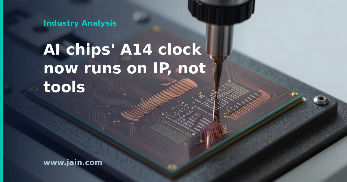
Before a new computer chip can be made, engineers draw and redraw its design in specialized software. Cadence, which makes that software, says its tools are now approved for the next, even smaller manufacturing process at Taiwan Semiconductor Manufacturing Company, the world’s biggest contract chipmaker.
Cadence says one tricky part of the job now needs up to two and a half times fewer redraws. That could speed up the custom artificial intelligence chips that giant cloud companies build. The catch: many ready-made parts Cadence sells for such chips are still unfinished, and some are not due until the end of this year.
Cadence Design Systems announced on September 23 an expanded partnership with TSMC, according to the company’s release as published by Wccftech. Cadence’s digital full flow, signoff flow and custom/analog flows are now certified for TSMC’s A16 and A14 process technologies, and its analog, digital and signoff flows are certified for N2P. Cadence says Virtuoso Studio’s automated layout generation and design migration to A16 and A14 reduces design iterations by up to 2.5x.
On intellectual property (IP) — pre-designed circuit blocks that chipmakers license rather than build themselves — Cadence reported a UCIe-64G chiplet interface taped out on A14, LPDDR6 memory-interface IP in development, and A14 foundation and mixed-signal IP expected in Q4 2026. It also cited support for TSMC’s SoW-X wafer-scale flow with hundreds of chiplets, a UALink demonstration on N3P, and design-services firm Global Unichip Corp. (GUC) as a customer.
Executive Summary
Tool certification is the gate that lets chip designers commit real products to a new manufacturing process. It means TSMC has validated Cadence’s software against its A14 and A16 design rules and models, so the layouts, timing and power numbers the tools produce can be trusted to match what the fab will build. Cadence has now cleared that gate for its digital, signoff and custom/analog flows on both nodes.
It matters because the next generation of custom AI accelerators — the chips hyperscalers design in-house to run alongside or instead of merchant GPUs — will migrate to these nodes, and the time between a node becoming available and silicon shipping in volume is set by tools, IP and packaging together. Cadence’s headline 2.5x figure is narrower than it first reads: it applies to automated custom and analog layout and migration, and it is stated as an upper bound.
The more consequential detail is in Cadence’s own status table. With tools certified, most of its A14 IP is still in development, with foundation and mixed-signal blocks due in Q4 2026. For design teams relying on that IP, the A14 schedule question has moved from software qualification to IP readiness. On the manufacturing side, TSMC’s latest 6-K shows its board approved US$16,035 million for advanced-technology capacity machinery in August — the fab is spending; design-side readiness determines how quickly customers can use it.
The 2.5x Applies to Analog Layout, Not the Whole Chip
Cadence ties its “up to 2.5X” reduction in iterations specifically to Virtuoso Studio’s design-rule-correct layout generation and automated design migration to A16 and A14 — the custom and analog side of the flow. Analog circuits handle continuous electrical signals rather than ones and zeros: the transceivers that move data off a chip, the physical interfaces to memory, clocking and power-management blocks. Digital logic can largely be re-mapped to a new node by synthesis and place-and-route software; analog layouts have traditionally been redrawn by specialists at each node, because exact transistor placement affects how the circuit behaves.
That makes analog a sensible target for automation. “Design-rule-correct” means the generated layout already obeys the foundry’s geometric rules on spacing and widths, cutting the draw-check-fix loop that consumes much of a migration. Shortening the workstream that scales worst with headcount is a real gain. But Cadence does not state the baseline — fewer iterations than which previous method, on which designs — and “up to” marks a best case. No comparable multiplier is claimed for the digital full flow, where most of an AI accelerator’s transistors sit.
For anyone estimating time to market, the 2.5x is a figure about iterations in one workstream, not a claim that chips ship 2.5 times sooner. Cadence’s own summary of the benefit — “faster time to market and improved PPA” (power, performance and area) — is not quantified.
Tools Are Certified; the A14 IP Ladder Is Still Being Climbed
Semiconductor IP climbs a ladder before customers trust it: designed, taped out (sent to the fab to make test chips), tested in the lab when silicon returns, then characterized — measured across voltage and temperature so its behavior is documented. Cadence’s UCIe-64G chiplet interface shows that ladder across nodes in a single announcement: characterized on N3P, in the lab on N2P, taped out on A14.
On A14 itself, the list is mostly future tense. UCIe-64G is taped out. LPDDR6 IP is in development. Artisan foundation IP — standard cells, the basic logic building blocks, plus GPIO and memory compilers — and mixed-signal IP are in development and expected in Q4 2026. Other HPC and AI memory IP and chiplet protocols have been “prioritized for development.” HBM4/4E and PCIe 7.0 appear in Cadence’s broader portfolio without an A14 status.
That is the mechanism behind the headline. A custom AI accelerator is mostly compute logic, but it cannot ship without the interfaces that connect it to high-bandwidth memory, sibling chiplets and the network — precisely the analog and mixed-signal blocks still in progress on A14. With certified tools in hand, a design team relying on Cadence’s A14 IP now faces a different schedule question: not whether the software is qualified, but when each block reaches proven silicon. Teams can source some blocks from TSMC or other IP vendors — Synopsys has announced its own TSMC partnership on agentic AI and advanced design — so this is a statement about Cadence-based flows and about where the gating item has moved, not a ceiling on the whole market.
Packaging Is Where the AI System Gets Assembled
The announcement gives as much space to packaging as to transistors. Cadence says its tools support TSMC’s SoW-X system-on-wafer flow with hundreds of chiplets and millions of bumps (microscopic solder connections), and CoWoS-L-style packages five times the reticle size. The reticle is the largest area a lithography scanner prints in one exposure, which effectively caps the size of a single die; a 5x-reticle package combines the silicon of several maximum-size dies in one module. A certified die-to-die auto-routing flow targets UCIe requirements across CoWoS architectures.
Cadence also cites TSMC-COUPE, a photonic engine that converts electrical signals to light close to the chip, enabled with its 224G SerDes IP and aligned with UALink, UltraEthernet, ESUN and co-packaged optics (CPO). These are the links that turn individual accelerators into clusters, and their readiness shapes what data center operators will be powering, cooling and cabling. Cadence discloses no power or thermal figures for these designs.
TSMC’s capital decisions point the same way. In a 6-K filed September 24, TSMC reported that its board approved US$16,035 million for advanced-technology capacity machinery, US$4,791 million for advanced packaging, mature and/or specialty capacity, and US$8,616 million for real estate and capitalized leased assets in August. The filing does not isolate packaging from the combined category or allocate spending by node, so it supports the direction of travel rather than any A14-specific conclusion.
Who Gains From Shorter Node Ramps
The most direct beneficiaries are the firms that build custom accelerators for hyperscalers. GUC, named as a customer, delivers custom silicon for AI accelerators and hyperscale systems on TSMC’s leading-edge nodes. Its senior vice president, Louis Lin, said success on N3P and N2P depends on tightly optimized execution, “especially when working with the early‑adopters where schedule risk is highest.” His remarks address N3P and N2P; the announcement names no A14 customer.
For hyperscalers, being early on a new node matters because each generation aims to deliver more computing per watt, which compounds across fleets of data center racks. But the constraints stack — certified tools, proven IP, packaging capacity, wafer capacity — and a design moves at the pace of the slowest. On A14, Cadence has cleared the first and is partway through the second.
Some claims need more support before buyers can weigh them: the UALink demonstration is described as “industry-leading” without published bandwidth, latency or power data, and “agentic AI chip design flows” are named but not defined. Both are marketing language until measured results follow.
Background
Chips are designed with electronic design automation (EDA) software — the programs engineers use to describe, lay out and verify circuits before a factory builds them. Cadence Design Systems and Synopsys are the two largest EDA suppliers, and both also license IP blocks such as memory and chiplet interfaces. TSMC, the largest contract chipmaker, manufactures chips designed by other companies, including many AI accelerators; its leading-edge roadmap runs from N3 and N2 to A16 and A14.
Every new process requires design tools and IP to be requalified before customers can commit products to it, which is why certification announcements cluster around each node. Hyperscalers increasingly design custom AI accelerators, often with design-services partners such as GUC, and those chips are now assembled from multiple chiplets in advanced packages — TSMC’s 3DFabric family, including CoWoS and SoIC — making packaging and die-to-die links as important to the schedule as transistor density.
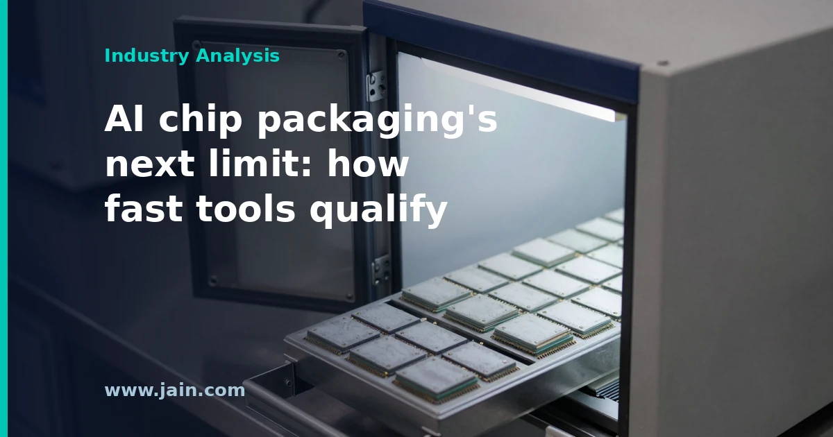
The chips behind AI tools like chatbots are not just manufactured. They are also assembled: several chips are placed side by side or stacked, then wired together into one package. How well that assembly works now affects how fast new AI chips can ship.
TSMC, the Taiwanese company that makes many of the world’s AI chips, is building a center in southern Taiwan to test new assembly machines and materials before they reach the factory floor. The goal is to catch problems early, instead of fixing them while production is already running.
Do not expect quick results. The center is due to open in late 2029.
Kaohsiung’s Baipu Industrial Park broke ground on September 21, 2026. SemiVision reported that TSMC will anchor the park with an advanced-packaging training and validation center. The center is not a production line. It is a facility where TSMC and its suppliers will jointly develop, test and qualify packaging equipment and materials. Earlier plans put TSMC’s initial site at roughly three hectares with two buildings, and operations are expected to begin around the fourth quarter of 2029.
The park covers about 88.7 hectares, including roughly 53 hectares of industrial land. Around 25 hectares of that are expected to focus on advanced back-end semiconductor equipment and related supply chains. Official estimates suggest the park could eventually generate around NT$300 billion in annual output and more than 4,000 jobs.
Executive Summary
TSMC’s Baipu center is built around a reconfigurable “Mini-Loop” validation platform. It will not house a complete CoWoS production line. Instead, selected process modules will be assembled, tested and swapped out as technologies change. CoWoS (Chip-on-Wafer-on-Substrate) is TSMC’s technique for placing an AI processor next to stacks of high-bandwidth memory (HBM) inside a single package, and it sits at the core of today’s AI accelerators.
The significance lies in what TSMC is separating out. It is moving equipment and materials validation out of its production fabs and into a dedicated site shared with suppliers. Validation is the work of proving that a new tool or material performs reliably enough for mass production. The move is a bet that AI chip supply increasingly depends on how quickly new packaging tools and materials can be qualified, and not only on how many packaging lines exist.
For suppliers, the promise is earlier entry into TSMC’s development cycle. For AI chip designers, the payoff, if it comes, is fewer surprises when new package designs reach volume production. Neither benefit is expected before late 2029.
Why the Gating Step Is Qualification Time, Not Floor Space
Front-end chipmaking, the step where transistors are patterned onto wafers, relies on equipment giants such as ASML, Applied Materials, Lam Research and Tokyo Electron. These companies run large R&D organizations and global field-service teams that help get new tools qualified. Advanced packaging has no equivalent bench strength. Many back-end equipment suppliers are much smaller, yet a long list of technologies is changing at the same time:
CoWoS itself
Hybrid bonding, which fuses chips copper-to-copper without solder bumps
Thermocompression bonding (TCB)
Temporary bonding and debonding
Wafer and panel handling
Automated optical inspection and metrology
Underfill, dielectric and thermal materials
The product cadence on top of that is accelerating. NVIDIA, AMD, Broadcom and custom AI chip (ASIC) developers keep introducing new architectures. HBM is moving from HBM3E toward HBM4 and beyond. Package size, die count, interconnect density and heat load are all rising together. The practical result is that one generation of equipment may not finish qualification before the next product generation arrives. Historically, some packaging tools were still being modified after installation, with engineers tuning them while production was already underway. A line that is being debugged is not yielding at full rate.
Baipu is TSMC’s structural answer: move troubleshooting upstream, so that equipment, material and integration problems surface before mass production. This is why capacity counts alone understate the constraint. A packaging plant full of tools that are not yet qualified for the next package design cannot ship the next accelerator. Two groups are most exposed. The first is accelerator designers, whose launch timing depends on new package formats. The second is smaller back-end toolmakers, who have lacked a place to prove their equipment at the pace TSMC’s customers now demand.
The Mini-Loop Is a Capital-Efficiency Choice
A fixed, full-scale experimental packaging line would require heavy capital expenditure. Because 3D IC, CoWoS, HBM and chiplet architectures are evolving quickly, that line’s configuration could be outdated within a few years. The Mini-Loop concept avoids this. TSMC brings in only the module that needs validating, tests it, modifies it, and then reconfigures for the next job. The validation infrastructure evolves with each technology generation instead of being written off along with the previous one.
The trade-off is fidelity. A modular loop tests modules. Some integration problems only appear when every step runs together at volume, and those may still surface in production. How much time Baipu actually saves will depend on two things: how TSMC bridges that gap, and whether validation results at Baipu carry directly into production qualification or must be partly repeated in the fabs.
From Equipment Vendor to Co-Development Partner
The conventional sequence runs like this: the customer sets a specification, the supplier builds the tool, the tool is installed in the fab, qualification begins, and then the equipment is modified in response to feedback. Baipu aims to put customers, equipment makers, materials companies and research organizations into the same development loop before mass production begins. In that loop, equipment fixes can happen immediately, and materials can move straight into another design of experiments (DOE, a structured test matrix). Software, automation, process recipes and metrology can all be tuned in parallel.
This is a different advantage from simple proximity. Being near TSMC saves shipping and service time. Entering its development cycle early lets a supplier help shape the specification instead of chasing it. The groundbreaking drew companies from across the stack: TSMC, ASE, Foxconn, ASPEED, WinWay, King Slide, Gudeng, C SUN, Grand Process Technology, Scientech, AblePrint, HIWIN and Gallant Precision Machining. Attendance does not confirm investment. The first phase is expected to include validation work linked to TSMC and its suppliers, along with Foxconn AI-related R&D and manufacturing. A later phase could support further advanced-packaging expansion, including requirements from companies such as ASE.
Kaohsiung presents Baipu as one link in a southern-Taiwan corridor:
Nanzih: advanced semiconductor manufacturing
Renwu: packaging and test
Ciaotou: materials and critical components
Gangshan and Lujhu: existing precision-machinery, metal-processing and fastener industries that the city hopes to pull into the equipment supply chain
If that works, the regional advantage would not rest on any single fab. It would rest on how tightly manufacturing, packaging, equipment and qualification can iterate over short physical distances.
What a 2029 Opening Means for Today’s AI Supply
With operations expected around the fourth quarter of 2029, Baipu sits outside the window of current packaging constraints. Tools and materials qualified there would serve product generations well beyond today’s HBM3E-based parts. Buyers of AI accelerators should not read Baipu as near-term relief. It is an investment in the rate at which packaging technology can change over the following years.
The headline economic figures are NT$300 billion in annual output and more than 4,000 jobs. These are park-wide official estimates, not TSMC commitments, and they say little about the metric that matters most to the industry: how much shorter qualification cycles actually become. No such target has been published. The argument that time-to-qualification is becoming the gating factor is coherent and fits the direction of packaging technology. Its payoff, however, will only be measurable in how many Baipu-validated tools reach production lines at TSMC, ASE or other manufacturers.
Background
TSMC (Taiwan Semiconductor Manufacturing Company) manufactures chips designed by other companies. In the AI era, its role has extended from wafer fabrication into advanced packaging. Packaging is the step where multiple chips, such as a processor and stacks of high-bandwidth memory, are combined into a single package. Technologies such as CoWoS, hybrid bonding and 3D IC stacking have made packaging a performance-critical part of AI accelerators, and HBM, substrates, thermal management, metrology and automation have become increasingly interdependent.
Southern Taiwan is a focal point of that build-out. Kaohsiung’s semiconductor base already spans Nanzih, Renwu and Ciaotou. The city is positioning Baipu Industrial Park, which broke ground in September 2026, as both an advanced semiconductor equipment and materials validation hub and an AI advanced-manufacturing base.
The chips that run artificial intelligence are not held up by the factories that print them. They are held up by the assembly step at the end, where a processor and its memory are bonded onto a single slab so they can talk to each other fast enough.
Taiwan Semiconductor Manufacturing Company owns most of the world’s capacity for that step. Analysts in Taiwan say it plans to roughly double that capacity by 2028. Until it does, anyone building an artificial intelligence data center is standing in a queue. Intel is selling a rival method, and smaller assembly firms are absorbing the overflow.
Wccftech, citing a Taiwanese media report that quotes analysts, said TSMC plans to expand its chip-on-wafer-on-substrate (CoWoS) advanced packaging capacity to 260,000 wafers per month by the end of 2028, roughly double the approximately 130,000 wafers per month the same forecast puts it at by the end of 2026. The expansion is said to center on TSMC’s Arizona campus and its AP7 packaging facility in Taiwan.
The same forecast estimates that Intel’s competing EMIB-T packaging, converted into CoWoS-equivalent 12-inch wafer terms, could reach 15,000 to 20,000 wafers per month in 2027 and 40,000 to 45,000 in 2028, and says the CoWoS shortage has pushed work toward other packaging firms including Amkor, UMC and ASE. TSMC has not published a capacity target of its own. In a Form 6-K filed with the Securities and Exchange Commission on September 10, the company reported August 2026 consolidated revenue of NT$514.81 billion, up 53.3 percent from a year earlier.
Executive Summary
Advanced packaging is the step where a logic die and its stacks of high-bandwidth memory are mounted together onto a shared substrate so they behave as one component. CoWoS is TSMC’s version, and it is the packaging used for the accelerators that fill AI data centers. For roughly three years it, rather than leading-edge wafer manufacturing, has been the narrowest point in the supply chain for those parts.
A doubling of that capacity by 2028 would be the single largest change to AI hardware availability that any one company can make. It would not, however, double accelerator output in a straight line. Package sizes are growing, the newest designs consume more interposer area and more memory stacks per unit, and a wafer of packaging substrate therefore yields fewer finished accelerators each generation than it did the year before. Capacity that doubles against demand that also rises per unit is not the same as supply that doubles.
TSMC’s own disclosure does not address packaging capacity. What its September 10 filing does show is demand running hot: August revenue rose 53.3 percent year over year, and revenue for the first eight months of 2026 was up 39.3 percent. That is consistent with a company selling everything it can finish, which is the condition under which a capacity forecast of this kind becomes credible without being confirmed.
The Bottleneck Moved Downstream
For most of the history of the chip industry, the scarce resource was the front end: photolithography tools, leading-edge wafer starts, yield on a new process node. Packaging was the cheap, unglamorous back end. AI accelerators inverted that. A modern accelerator is not one chip but an assembly, a large logic die surrounded by stacks of memory, all sitting on a silicon interposer threaded with vertical connections called through-silicon vias. The density of those connections is what delivers the memory bandwidth the workload needs. That assembly step is CoWoS, and there is no abundant substitute for it.
The practical consequence for anyone financing a data center is that wafer capacity is no longer the number to watch. A foundry can start more wafers than it can finish into packages, and unfinished silicon does not train models. The forecast of 130,000 wafers per month at the end of 2026 rising to 260,000 by the end of 2028 is, in effect, a two-year schedule for how quickly the industry can convert build-ready halls into loaded racks.
Read it with care, though. Interposer area per accelerator has been climbing with every generation as designers add memory stacks and reticle-stitched logic. If the average package consumes meaningfully more of a wafer in 2028 than it does today, unit output grows by considerably less than the wafer count suggests. Doubling the input is a ceiling on supply growth, not a promise of it.
Arizona Can Print the Chips but Cannot Finish Them
The most operationally interesting detail in the forecast is geographic. Wafers produced at TSMC’s Arizona campus are flown to Taiwan to be packaged, because the packaging capacity sits on the island. Siting part of the expansion in Arizona alongside the AP7 facility in Taiwan would begin to close that loop, turning an American fab from a wafer source into something closer to a finished-component source.
That matters for reasons beyond logistics. A round trip across the Pacific adds days of cycle time and a customs and freight cost to every high-value wafer, and it means that the resilience argument for building fabs outside Taiwan is currently incomplete. A domestic fab whose output must still transit Taiwan to become a usable product does not remove the concentration risk that justified it. TSMC’s own filing shows the Arizona entity is treated as a significant subsidiary, with parent guarantees extended to TSMC Arizona among other affiliates, but the filing says nothing about packaging there.
For data center operators and the governments underwriting them, this is the question worth asking of any onshoring announcement: does the site produce a wafer or a shippable part? Until packaging follows fabrication, the answer for Arizona remains the former.
Intel’s EMIB-T and the Value of a Second Source
Intel’s EMIB-T takes a different architectural route. Instead of building the whole assembly on a large silicon interposer, it embeds small silicon bridges inside the organic substrate and places the logic and memory dies on top. Less silicon is used, which can mean lower cost and fewer of the handling and warpage problems that come with very large interposers, but the approach historically trades away some of the interconnect density that the largest, most bandwidth-hungry designs demand.
The forecast puts EMIB-T at 40,000 to 45,000 CoWoS-equivalent wafers per month by 2028. Against 260,000, that is a meaningful second source rather than a competitive threat, on the order of a sixth of the leader’s volume. The claim that it suits custom accelerators of the kind Google and Amazon design is plausible on architecture, since in-house cloud silicon is generally tuned for a known workload and a known cost target rather than for maximum bandwidth per package. It is also unverified: neither Intel nor any cloud provider has announced such an arrangement.
The spillover to Amkor, UMC and ASE follows the same logic. When the preferred supplier is sold out, work migrates to whoever can perform an adjacent version of it, and outsourced assembly and test firms have been the natural landing place. Buyers get optionality and a check on pricing. The risk is that second-source packaging is not a drop-in substitute. Requalifying a part on a different packaging architecture is an engineering program, not a purchase order, and the customers best placed to do it are the ones designing their own silicon.
What Is Substantiated and What Is Not
The demand side of this story rests on disclosed figures. TSMC’s September 10 filing with the Securities and Exchange Commission reports August consolidated revenue of NT$514.81 billion, a 10.1 percent increase on July and 53.3 percent on August 2025, with the first eight months of 2026 up 39.3 percent year over year. Growth at that rate at TSMC’s scale is difficult to explain without sustained AI accelerator demand behind it.
The supply side is a forecast, not a commitment. The 260,000 figure, the 130,000 baseline, the Arizona and AP7 split and the EMIB-T range all come from analysts rather than from the companies. None of the three firms named has published a packaging capacity target, a capital budget attached to one, or a schedule. Analyst capacity models in this industry have a reasonable track record on direction and a poorer one on timing, because packaging expansions depend on tool delivery, cleanroom construction and qualification cycles that slip quietly.
The sober reading is that the direction is well supported and the magnitude is an estimate. Treat 2028 as the earliest plausible date for materially looser accelerator supply, treat the doubling as a ceiling rather than a plan of record, and treat any procurement model that assumes it as carrying schedule risk that TSMC has not underwritten.
Background
TSMC is the world’s largest contract chip manufacturer, building processors designed by other companies. It commercialised CoWoS in the 2010s as a niche technique for high-performance parts, long before AI accelerators turned it into the scarcest resource in the industry. Today the packaging step determines how many finished accelerators reach the market, because a logic die without its memory bonded alongside it is not a usable product.
The competitive response has come from two directions. Intel has pushed its own bridge-based packaging as part of its foundry ambitions, targeting customers who want a supplier outside Taiwan or a lower-cost assembly for custom silicon. Outsourced assembly and test firms such as Amkor, ASE and UMC have absorbed work that TSMC cannot schedule. None of this has yet changed the basic shape of the market, in which one company’s packaging line sets the pace at which AI data centers can be filled.
Almost all of the advanced chips that make artificial intelligence work are built by one company in Taiwan. In August it sold roughly 16 billion US dollars’ worth in a single month, more than half again what it sold in the same month a year earlier.
This matters to anyone outside the industry because the huge computing warehouses being built around the world cannot switch on without those chips. The buildings can go up fast. The chips cannot.
So the real waiting line for artificial intelligence computing now begins long before anyone pours concrete.
Taiwan Semiconductor Manufacturing Company (TWSE: 2330, NYSE: TSM) reported consolidated net revenue of approximately NT$514.81 billion for August 2026, up 10.1 percent from July and 53.3 percent from August 2025, according to the revenue report the company filed with the US Securities and Exchange Commission on Form 6-K on September 10. Revenue for January through August 2026 totalled NT$3,386.87 billion, a 39.3 percent increase over the same period in 2025.
The August figure sits roughly 22 percent above the company’s average month so far this year, and its year-over-year growth rate runs well ahead of the 39.3 percent pace of the eight-month total, meaning growth is accelerating rather than merely continuing. Benzinga reported that August marked a fourth consecutive month of revenue growth, that TSMC raised its 2026 capital spending plan in July to a record US$60 billion to US$64 billion, that second-quarter revenue rose 36 percent year over year to NT$1.27 trillion, and, citing research firm TrendForce, that TSMC held 72.5 percent of the global foundry market in the second quarter with its 5, 4 and 3 nanometre capacity fully booked on demand for AI server processors.
Executive Summary
A single month of revenue from one Taiwanese manufacturer has become one of the more reliable read-throughs on the health of global AI infrastructure spending. TSMC is a foundry, meaning it does not design chips but manufactures them for companies that do, including the accelerator vendors whose parts fill AI data centres. When its monthly revenue accelerates to 53.3 percent growth, the most direct interpretation is that customers are taking every wafer they can get, and that the manufacturer is able to price and mix accordingly.
The strategic point for infrastructure buyers is where the queue actually forms. Public debate about AI capacity has centred on land, grid interconnection and cooling, all of which are genuine constraints. But a rack cannot be commissioned without accelerators, and accelerators cannot be finished without leading-edge wafers and the advanced packaging that bonds those wafers to high-bandwidth memory. Capacity at the leading edge is described as fully booked. That places the tightest link in the chain upstream of anything a data centre developer controls.
The second implication is financial. TSMC lifted its 2026 capital budget to a record range in July while continuing to distribute cash, adjusting its first-quarter dividend to NT$7.00000137 per common share for payment on October 8 in a separate 6-K filed on September 1. Spending at that scale is a multi-year commitment made against demand signals that are, so far, monthly. The capacity being funded now will arrive after the current shortage, which is the central risk in any capital cycle built on scarcity.
The Constraint Has Moved From Buildings to Wafers
For most of the last two years, the limiting factor discussed in data centre planning has been physical and local: available land, transformer lead times, water for cooling, and the interconnection queue, the waiting list operators join to connect a large load to the electricity grid. Those constraints have not eased. What August’s number suggests is that they now share the critical path with something further upstream, and less visible from the site fence.
An AI accelerator is not a single piece of silicon. It is a leading-edge logic die manufactured on a 3 or 4 nanometre process, joined to stacks of high-bandwidth memory through advanced packaging, a set of techniques that place multiple dies on a shared substrate so they can exchange data at speeds a conventional package cannot support. Packaging capacity is a separate physical constraint from wafer capacity, built in different buildings on different timelines. A shortage in either one caps finished accelerator output regardless of how many wafers the fabs can start.
That is why a foundry’s revenue line has become a leading indicator for facilities that will not open for another two years. If leading-edge capacity is fully booked, as reported for the second quarter, then the marginal buyer of AI compute is not competing for megawatts alone. They are competing for an allocation that was effectively decided upstream, months before their building was energised.
Reading a Monthly Number Without Overreading It
Monthly revenue is a coincident indicator, not a forecast. It records wafers shipped and recognised now, from orders placed and started months earlier. A strong August therefore confirms that demand was strong in the spring and early summer. It does not, by itself, tell you what the order book looks like for the second half of 2027, which is the period most relevant to infrastructure now under construction.
Two further cautions apply to the headline growth rate. The first is the comparison base: a 53.3 percent increase is measured against August 2025, and the strength of that month shapes the number as much as the strength of this one. The second is currency. TSMC reports in New Taiwan dollars, so any US dollar figure quoted alongside it moves with the exchange rate, and dollar-denominated growth can differ from the reported figure in either direction. The 10.1 percent sequential rise from July is in some ways the cleaner signal, because it compares two adjacent months on the same basis and is unaffected by what happened a year ago.
What the monthly disclosure does not contain is mix. It is a consolidated total, without a breakdown by process node, end market or customer. The attribution of the growth to AI is an inference drawn from the pattern of demand, from the reported utilisation of the advanced nodes, and from the second-quarter commentary about a multi-year infrastructure build-out. It is a well-supported inference. It remains an inference, and readers should hold it as one.
A Record Capital Budget Is a Bet That Demand Persists
The July decision to raise 2026 capital spending to a record US$60 billion to US$64 billion is the more consequential disclosure for the industry, because it determines what supply looks like in 2028 and 2029. Fabs take years to build, qualify and ramp. Capital committed during a shortage arrives, almost by definition, into a different market than the one that justified it. This is the oldest dynamic in semiconductors, and it has produced both the industry’s great expansions and its sharpest downturns.
The September filing offers an incidental view of how that expansion is being carried. Alongside the revenue table, TSMC discloses funds lent to TSMC Washington and guarantees extended to TSMC North America, TSMC Global and TSMC Arizona, all wholly-owned subsidiaries. Overseas manufacturing is being financed and backstopped from the parent balance sheet rather than standing on its own. For customers concerned about geographic concentration of leading-edge supply, that structure is worth understanding: diversification of sites does not by itself diversify the credit or the operating control behind them.
Capital returns are running in parallel. The dividend adjustment filed on September 1 reset the first-quarter distribution to NT$7.00000137 per common share, a technical correction after shares were reclaimed from 2024 restricted stock awards, payable on October 8. The approved distribution of roughly NT$181.5 billion for a single quarter is equivalent to about a third of one strong month’s revenue. A company financing record capacity expansion while sustaining distributions of that size is signalling confidence in cash generation, not merely in demand.
What Buyers of Compute Should Take From This
For enterprises procuring AI capacity, whether as hardware or as cloud instances, the practical lesson is that allocation risk sits upstream of the vendor they negotiate with. If accelerator supply is rationed at the foundry and packaging stage, then delivery commitments from any intermediary inherit that scarcity. The right questions in a procurement conversation are about the supplier’s own allocation and its timing, not only about their willingness to sign a schedule.
For operators and developers, the sequencing implication cuts both ways. A site that lands power and interconnection early but cannot secure silicon carries stranded capital in the form of an energised shell with nothing to run. A site with committed accelerators and no grid connection carries the mirror-image problem. The scarce resources are complementary and their lead times are not synchronised, which argues for procuring them against each other rather than in sequence.
For investors, concentration is the theme worth tracking. A reported 72.5 percent share of global foundry revenue in the second quarter, with the leading-edge nodes described as fully booked, means one manufacturer’s throughput is a meaningful variable in the capital plans of the largest technology firms in the world. That is a strong commercial position and, simultaneously, a systemic dependency. Both readings are true, and the numbers above support each.
Background
TSMC pioneered the pure-play foundry model after its founding in 1987: rather than designing and selling its own chips, it manufactures to order for companies that design them. That model now underpins most of the semiconductor industry, because building a leading-edge fab costs tens of billions of dollars and only a handful of firms can operate at the front of the process roadmap. Process generations are named for nominal feature size, with 3 nanometre currently at the leading edge, 4 and 5 nanometre one step behind, and older nodes still serving automotive, industrial and consumer parts.
Because it is listed in Taipei, TSMC discloses revenue every month, a cadence rare among large manufacturers elsewhere and one reason its figures are watched as a proxy for global chip demand. The same report is filed with the SEC on Form 6-K, which is how US investors receive it. Since AI accelerators became the industry’s dominant growth driver, these monthly disclosures have functioned as a near-real-time gauge of how fast the AI infrastructure build-out is actually consuming silicon.
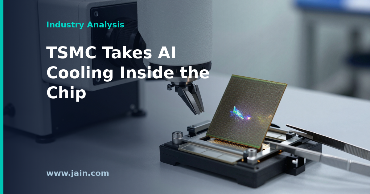
The chips that run artificial intelligence are getting so hot that cooling them from the outside is starting to run out of room. TSMC, the Taiwanese company that manufactures most of the world’s advanced processors, is looking at cutting channels finer than a human hair into the chip itself and pumping liquid through them, right next to where the heat is made.
Forecasts put the power a single artificial intelligence system draws at roughly six times today’s level within five years. If cooling moves inside the chip, the company that builds the chip starts selling the cooling too.
TrendForce reported that TSMC is evaluating microchannel cooling integrated at the chip level — etching or bonding fluid channels directly into the silicon package so coolant flows microns from the transistors — as projected power draw for AI systems rises roughly sixfold over the next five years. The report frames the technology as a response to the point at which conventional external cooling, including metal cold plates strapped to the top of a processor, stops keeping pace with heat generated inside the package.
TSMC has not addressed the technology in its recent filings with United States regulators. Its 6-K filed August 25, 2026 covering July activity reported no board-approved capital appropriations for the month, and its 6-K filed September 1, 2026 dealt with a routine dividend adjustment.
Executive Summary
For a decade, cooling improvements in computing happened outside the chip: better fans, then cold plates, then facility water loops and immersion tanks. Chip-level microchannel cooling breaks that pattern. It puts the coolant inside the package itself, shortening the path heat must travel from transistor to fluid — the single largest source of thermal resistance in a modern accelerator stack. If TSMC productizes it, cooling stops being purely a data center purchase and becomes partly a foundry and advanced-packaging purchase.
The sixfold power projection is the forcing function. Each generation of AI accelerator has raised per-package power while shrinking the area over which that heat can be spread. External cooling can move more fluid faster, but it cannot shorten the distance between the hot spot and the fluid. Microchannels can, which is why the approach has moved from research curiosity toward roadmap discussion.
The commercial implications run in several directions at once: advanced packaging gains value, cold-plate and thermal-interface suppliers face a long-run substitution question, and data center operators inherit a component that is sealed, unserviceable and warranted by the chipmaker rather than the integrator. None of that is settled, and TSMC has published no timeline, node, capacity or customer detail.
Why the Thermal Bottleneck Has Moved Below the Heatsink
Heat leaving a processor passes through a chain of obstacles: the silicon itself, a thermal interface material, a metal lid, another interface layer, and finally a cold plate or heatsink carrying the heat away. Each junction adds resistance. Data center engineering over the past few years has attacked the last link in that chain — swapping air for water, moving from rear-door heat exchangers to direct-to-chip cold plates, adding coolant distribution units. Those changes worked, but they optimise the part of the path furthest from the problem.
Microchannel cooling attacks the first link. By routing fluid through channels formed in or immediately against the silicon, it removes several interface layers and places coolant adjacent to the hot spots rather than millimetres above them. That matters most for the tightly packed, high-power dies used in AI training accelerators, where heat is not evenly distributed and a small area of the die can limit the performance of the whole package.
The projected sixfold rise in AI system power over five years is what makes this urgent rather than academic. Cooling capacity outside the package can be scaled by spending more — bigger pumps, colder water, more plumbing. Thermal resistance inside the package cannot be spent away. Once it dominates, the only remaining lever is to redesign the package, which is precisely where a foundry with leading advanced-packaging capability has an advantage.
Cooling Becomes a Foundry Product
The business consequence is a shift in where cooling value is captured. Today a hyperscaler — an operator of very large cloud data centers — buys accelerators from a chip designer and cooling from a separate thermal supply chain of cold-plate makers, manifold vendors, pump and coolant distribution unit manufacturers. If the highest-value part of the thermal path is fabricated at the packaging stage, part of that spend migrates upstream into the price of the package.
That is a favourable structural position for TSMC, which already assembles AI accelerators using advanced packaging that stacks logic dies and high-bandwidth memory on a shared substrate. Adding fluid channels to that flow extends an existing chokepoint rather than opening a new competitive front. For established thermal suppliers, the risk is gradual rather than immediate: facility-side cooling, plumbing and heat rejection remain necessary regardless, because heat still has to leave the building. What could shrink is the premium attached to the interface between chip and coolant.
There are real costs on the other side of the ledger. A sealed fluid path inside a package is not field-serviceable. Leaks, corrosion, particulate clogging and mechanical stress become manufacturing yield and warranty problems for the chipmaker rather than maintenance problems for the operator. Testing a package that only performs correctly when fluid is flowing complicates production test. Those are engineering problems with known research literature behind them, but solving them at high volume and acceptable yield is a different exercise from demonstrating them.
What TSMC’s Filings Do and Do Not Show
TSMC’s recent disclosures to United States regulators contain nothing about the technology. The 6-K filed on August 25, 2026, which reports the company’s July activity, listed no capital appropriations approved by the board that month, recorded a NT$0.7 billion equity investment disposition, and reported no share pledges or cancellations. The 6-K filed on September 1, 2026 was narrower still: an adjustment of the first-quarter 2026 cash dividend from NT$7.0 to NT$7.00000137 per common share, payable October 8, 2026, after shares were reclaimed from 2024 restricted stock awards.
This absence is not evidence against the programme. Research and early development work does not normally surface in monthly shareholding and appropriation reports, and companies routinely discuss roadmap directions publicly long before they appear as line items. But it does bound what can currently be said: there is no disclosed capital commitment, no announced capacity, and no financial scale attached to chip-level cooling at TSMC.
For investors, that suggests where to look next rather than what to conclude now. Board-approved capital appropriations in the monthly filings, advanced-packaging capacity announcements, and any customer disclosure from accelerator designers would be the first hard signals that microchannel cooling has moved from evaluation to committed investment.
What It Changes for Data Center Buyers — and What It Doesn’t
Operators planning liquid-cooled halls should not read this as a reason to wait. Chip-level cooling reduces resistance inside the package; it does not eliminate the need for a facility water loop, coolant distribution units, heat rejection equipment or the electrical capacity to feed the racks. If anything, a package designed to shed more heat more efficiently makes the facility-side loop more important, because more watts per rack must ultimately be rejected to air, water or the outside environment.
The more consequential change is contractual. Cooling that ships inside the processor moves specification authority to the chipmaker: coolant chemistry, filtration standards, inlet temperature and flow requirements would become conditions of the chip’s warranty rather than choices made by the integrator. Operators used to negotiating thermal design with a systems vendor may find those parameters arriving pre-set.
None of this is imminent. What the direction of travel does justify is designing new capacity for liquid distribution and water quality management as a baseline rather than an upgrade, since every plausible version of the next five years — cold plates, microchannels or both — ends with liquid at the rack.
Background
TSMC is the world’s largest contract chip manufacturer, producing leading-edge processors for companies that design but do not fabricate their own silicon. Its role in AI hardware extends beyond making transistors: its advanced packaging capacity, which bonds logic dies and high-bandwidth memory onto a shared substrate, has been one of the industry’s tightest bottlenecks through the current build-out. As a foreign private issuer listed in New York, TSMC files monthly 6-K reports with United States regulators covering board capital appropriations, asset transactions, bond issuance and insider shareholdings.
Cooling has escalated in parallel. Air cooling gave way to rear-door heat exchangers, then to direct-to-chip cold plates and facility water loops as accelerator power outgrew what fans could handle. Each step moved the working fluid closer to the processor while leaving the package itself untouched. Chip-level microchannel cooling is the logical next step in that sequence — and the first one that would be manufactured by the chipmaker rather than installed by the data center.