Category: AI Infrastructure

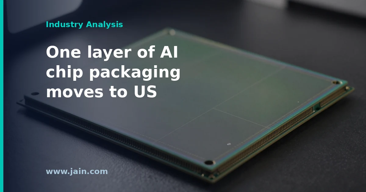
  • A $2B GlobalFoundries-TSMC Deal Onshores AI’s Interposer, Not the Whole Package

    A $2B GlobalFoundries-TSMC Deal Onshores AI’s Interposer, Not the Whole Package

    TL;DR · 30-second read

    The Short Version

    Two major chipmakers, GlobalFoundries and Taiwan Semiconductor Manufacturing Company, the world’s largest contract chipmaker, have struck a $2 billion deal to make a key chip part in the United States.

    The part is a silicon “interposer”: a thin slab of silicon that sits under an artificial intelligence processor and wires it to its memory, like a shared floor both chips are mounted on. The packaging step built around it has been one of the main limits on how many artificial intelligence chips get shipped.

    Making it in America could add supply outside Taiwan. But it covers one step, not the whole chip.

    Yahoo Finance reported that GlobalFoundries and TSMC have reached a $2 billion deal for silicon interposers produced in the United States. Silicon interposers are the base layer in the advanced packages that join high-end AI processors to stacked high-bandwidth memory, which places the agreement inside the part of the GPU supply chain that has repeatedly constrained output.

    The deal follows TSMC’s October 8 Form 6-K, its September 2026 revenue report, which showed consolidated revenue of roughly NT$511.86 billion for the month, up 54.6 percent from September 2025, and NT$3,898.73 billion for January through September, up 41.1 percent year over year.

    Executive Summary

    The headline facts are simple: a $2 billion agreement between the world’s largest contract chipmaker and a US-headquartered specialty foundry, covering a component that is made in the United States. The interposer is not a commodity part. It is a large piece of silicon, patterned in a wafer fab with fine wiring and vertical connections called through-silicon vias. AI accelerators mount their compute die and memory stacks on it side by side.

    That matters because AI chip supply has been gated less by the ability to make processors than by the ability to package them with memory. Making interposers in the US adds a domestic source for one input to that packaging flow. However, an interposer is an intermediate part. Until the companies say where the rest of the package is assembled, the deal shows where part of the bottleneck can be relieved, not that it has been.

    For GlobalFoundries, a $2 billion commitment tied to AI packaging is a significant new line for a foundry that stepped back from the leading-edge process race in 2018. For TSMC, whose September revenue alone was more than NT$500 billion, the deal is small in financial terms. Its importance is geographic and logistical.

    Why the Interposer Sits on AI’s Critical Path

    The most capable AI accelerators are not a single chip. They are assemblies. A large processor die sits next to several stacks of high-bandwidth memory (HBM), DRAM chips stacked vertically to deliver very fast data access. These parts have to talk to each other across thousands of extremely fine connections, far denser than an ordinary circuit board can carry. The silicon interposer solves this. It is a slab of silicon wired with lithography, the same patterning process used to make chips, so the processor and memory can be packed millimetres apart and connected at chip-level density.

    TSMC’s version of this approach is CoWoS, short for chip-on-wafer-on-substrate. Dies are bonded onto an interposer wafer, which is then mounted on a conventional package substrate. In recent years, CoWoS capacity has been widely identified as a binding constraint on AI accelerator shipments. The processors could be fabricated, but there was not enough capacity to package them with their memory. Interposers are one input to that flow. Because they are made in a fab rather than an assembly house, adding interposer supply requires wafer capacity with the right tooling, not just more packaging lines.

    What Onshoring One Layer Does, and What It Doesn’t

    This is the substance behind the headline. A US-based interposer source moves one fab-made step of AI packaging onto American soil. That has real value. It adds a source outside Taiwan for a component tied to a known chokepoint. It suits a mature, non-leading-edge process, which plays to GlobalFoundries’ strengths in its New York and Vermont fabs. It also gives chip designers and their hyperscale customers, the largest cloud and AI operators, a domestic option to cite when they are asked about supply resilience.

    But an interposer alone does not make a finished accelerator. After the interposer is made, the processor dies and memory stacks must be bonded onto it. The assembly must then be mounted on a substrate, tested, and shipped. If those steps remain in Taiwan, US-made interposers simply cross the Pacific in the opposite direction from the processors. Much of the processor output from TSMC’s Arizona fabs has itself needed to return to Taiwan for advanced packaging. The deal becomes a genuinely domestic AI supply chain only when it pairs with US assembly capacity. TSMC said in March 2025 that its expanded Arizona plans include advanced packaging facilities, and its October 6-K shows continued financial support for US subsidiaries, recording lending to TSMC Washington and guarantees for TSMC Arizona. Connecting the interposer supply to that assembly capacity is the step that would turn a single onshored layer into an onshored package.

    The packaging variant also matters. TSMC’s family includes the original CoWoS-S, which uses a full silicon interposer, and newer variants such as CoWoS-L, which replace the full interposer with smaller embedded silicon bridges. If flagship accelerators continue shifting toward bridge-based designs, the market for full-size interposers looks different. Which products these US interposers serve will determine how much of the bottleneck they actually touch.

    Reading $2 Billion Against Each Company’s Scale

    For TSMC, the figure is modest. Its September revenue was about NT$511.86 billion, and its year-to-date revenue was NT$3,898.73 billion, up 41.1 percent. A $2 billion agreement is not a material financial event at that scale. It is a capacity and location decision. Choosing a domestic partner for a mature-process component frees TSMC to focus its own capital elsewhere while adding a US element to its packaging chain.

    For GlobalFoundries, the calculus runs the other way. A foundry that chose in 2018 to stop pursuing the most advanced process nodes now has a direct line into the most supply-constrained segment of the AI hardware market, using processes it already runs. That makes it a significant win, though its annual revenue impact cannot be assessed until the contract’s duration and ramp are known. The two companies were once adversaries in a patent dispute that they settled in 2019 with a broad cross-license. A supply relationship on AI packaging is a notable evolution from that history.

    Background

    TSMC, founded in Taiwan in 1987, is the world’s largest contract chipmaker. It manufactures processors for most leading AI chip designers, and its CoWoS packaging has become central to AI accelerator supply. It is building fabs in Arizona and has said its US plans include advanced packaging. GlobalFoundries, spun out of AMD in 2009, runs fabs in Malta, New York; Essex Junction, Vermont; Dresden; and Singapore. It stopped pursuing the most advanced process nodes in 2018 to focus on specialty technologies.

    The two companies settled a patent dispute in 2019 with a broad cross-license. Their new interposer agreement places GlobalFoundries’ US mature-process capacity inside the AI packaging flow that TSMC dominates.

    Sources

    Source: GlobalFoundries and TSMC reach $2B deal for US-based silicon interposers (Yahoo Finance): report of a $2 billion agreement covering US-made silicon interposers.

    Primary sources: Taiwan Semiconductor Manufacturing Company, Form 6-K filed 2026-10-08 (TSMC September 2026 Revenue Report).

  • $2.5B AI Server Diversion Plea Tests Export Controls Where GPUs Become Servers

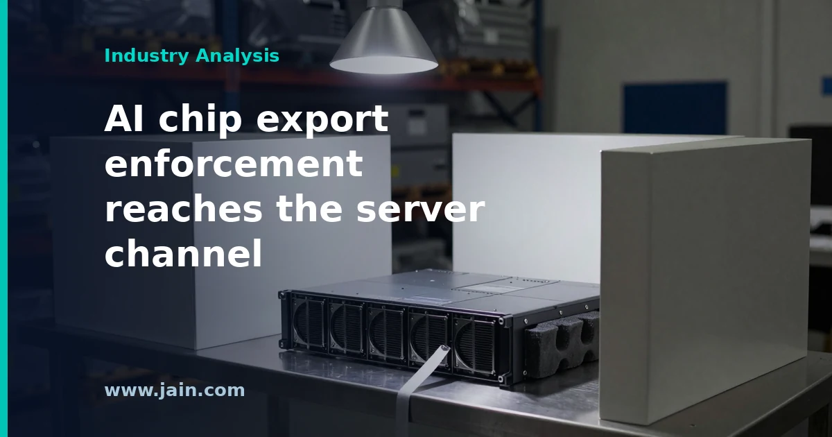
    $2.5B AI Server Diversion Plea Tests Export Controls Where GPUs Become Servers

    TL;DR · 30-second read

    The Short Version

    A contractor who worked with Super Micro, an American company that builds the powerful computers used to run artificial intelligence, has admitted in court to helping send those machines to China illegally. The scheme was valued at $2.5 billion.

    The computers held chips from Nvidia, whose chips power much of today’s AI. US rules bar selling those advanced chips to China without government permission.

    Why it matters: the case targets the people between the chipmaker and the final buyer, not the chipmaker itself. Enforcement is reaching further down the supply chain.

    A contractor tied to Super Micro Computer has pleaded guilty in a scheme to divert AI servers containing Nvidia chips to China, Reuters reported. Coverage puts the scheme’s value at $2.5 billion and describes the contractor as a co-defendant of a Super Micro co-founder.

    The plea comes in the same week Super Micro disclosed board changes in an 8-K filed October 8. That filing does not mention the export case.

    Executive Summary

    A guilty plea in a $2.5 billion AI server diversion scheme is among the clearest signals yet of where US export-control enforcement on AI hardware is landing. The equipment at issue was not loose chips but complete servers built around Nvidia GPUs (graphics processing units, the processors that do most AI computation). The person admitting guilt is a contractor, not an employee of the chipmaker.

    That matters because it shifts the compliance burden. Export restrictions on advanced AI chips follow the chip into whatever system it is installed in. That makes everyone who builds, resells or ships those systems a potential point of failure, and of liability. For server makers, distributors and the data center operators who buy from them, the case is a reminder that end-user screening is part of the product, not paperwork around it.

    The plea establishes guilt only for the person who entered it. Anything alleged against other defendants remains an allegation, and no charges against Super Micro as a company have been reported.

    Where a GPU Becomes a Server, Control Gets Harder

    Advanced AI chips leave Nvidia in large, traceable allocations to a relatively small set of server makers and cloud buyers. Once a GPU is installed in a server, it becomes one component inside a finished system. That system can then pass through distributors, contractors and resellers before reaching its final operator. US export rules still apply to the chip inside the box, but the chipmaker’s line of sight usually ends at its direct customer.

    That gap is the mechanism this case exposes. The diverted goods were Super Micro AI servers with Nvidia chips inside, and the guilty party is a contractor in the server maker’s orbit. At a reported $2.5 billion, the scheme shows how much hardware value can move through the integration and resale layer, the stage after the chip is sold but before the system is plugged in. Controls written around the chip are only as strong as the checks at that downstream stage.

    Those affected are the companies that sit between foundry and data hall: server builders, value-added resellers, logistics contractors, and the compliance teams that sign off on who the end user really is. Nvidia’s chips were in the boxes, but Nvidia is not reported to be a defendant and has made no material SEC filing on the matter. The enforcement weight in this case sits downstream.

    What the Channel Now Has to Prove

    For server makers and their partners, export compliance means knowing the end user and the end use, not just the immediate buyer. A diversion scheme works by putting a permissible-looking customer between the seller and a prohibited destination. A plea at the contractor level gives every company in that chain reason to scrutinize intermediaries, shipping patterns and resale terms more closely.

    The economic effect is friction. Legitimate buyers of AI servers, from enterprise IT departments to colocation tenants, may face more documentation about where systems will be deployed and who will operate them. For integrators competing on speed of delivery during a GPU supply crunch, slower deal reviews carry a real cost. The case makes clear that the alternative cost is higher.

    What Is and Isn’t Established About Super Micro

    Super Micro is one of the largest builders of Nvidia-based AI servers, so any case involving its products draws attention to the company. The facts on the record are narrower than the headlines. A contractor has admitted guilt. A co-founder is described as a co-defendant, which is an allegation, not a finding. No charges against the company have been reported.

    Super Micro’s most recent disclosure is an 8-K covering the appointment of former Intel IT chief technology officer Shesha Krishnapura as an independent director and the retirement of director Judy Lin. The filing states that Lin’s departure was not the result of any disagreement with the company, and it does not reference the case. Reading a connection into the timing would go beyond what either the plea or the filing supports.

    Background

    Since 2022 the United States has restricted exports of advanced AI chips and the systems built around them to China, through rules administered by the Commerce Department’s Bureau of Industry and Security and tightened in later rounds. Nvidia, the dominant supplier of AI accelerators, sells its GPUs largely through server makers and large cloud buyers, which turn them into finished systems.

    Super Micro Computer, based in San Jose, California, is one of the biggest of those server makers and a major builder of Nvidia-based AI systems for data centers. Its fiscal year ended June 30, 2026. In early October it announced a board change, adding former Intel IT chief technology officer Shesha Krishnapura and accepting the retirement of director Judy Lin.

    Sources

    Source: Super Micro contractor pleads guilty in scheme to divert AI servers with Nvidia chips to China (Reuters via Investing.com): a contractor pleads guilty in a reported $2.5 billion scheme to divert Nvidia-equipped AI servers to China.

    Primary sources: Super Micro Computer, Form 8-K filed October 8, 2026 (board appointment of Shesha Krishnapura and retirement of Judy Lin).

  • CoreWeave’s 15x Reload Claim Puts AI Inference on the Training Critical Path

    CoreWeave’s 15x Reload Claim Puts AI Inference on the Training Critical Path

    TL;DR · 30-second read

    The Short Version

    CoreWeave is a company that rents out the powerful computer chips used to build artificial intelligence. It has now launched Forge, a software toolkit for building and running artificial intelligence systems. Anyone can start using it for free.

    The surprising part: when these systems learn by trial and error, they keep swapping in updated versions of themselves. CoreWeave says it made that swap 15 times faster in testing, so the learning stops stalling.

    The move also puts CoreWeave in more direct competition with Amazon, Google and Microsoft, which already sell similar toolkits.

    CoreWeave has launched CoreWeave Forge, a platform that connects model serving, observability, post-training and evaluation in one environment. It was unveiled at the Fully Connected event and is free to start, with paid tiers for additional capabilities. CoreWeave’s product page describes Forge as a way to “run, observe, curate, improve, and evaluate models and agents” without locking work to one cloud, model or framework.

    SiliconANGLE reported on October 8 that Urvashi Chowdhary, CoreWeave’s vice president of product and AI services, said a preview capability called CoreWeave RL Rollouts, built on Nvidia’s Dynamo framework, improved model reload latency by 15x compared with a baseline configuration in testing.

    Executive Summary

    CoreWeave built its business renting GPU capacity, the graphics processors that train and run AI models. Forge adds managed software on top of that capacity. According to CoreWeave’s product page, it covers fine-tuning, managed reinforcement learning, per-token serverless inference, dedicated inference, agent tracing, sandboxes, a model and dataset registry, and experiment tracking through Weights & Biases Models. The free entry tier extends the platform to individual developers, not only the large labs and enterprises that sign capacity contracts.

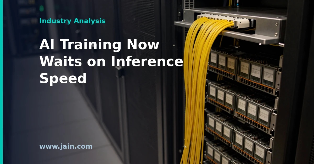
    The most technically significant claim concerns reinforcement learning, the training method used to build agentic models that take multistep actions. In that workflow, the inference system that generates the model’s attempts has to keep reloading freshly trained versions of the model. CoreWeave says RL Rollouts cut that reload time 15-fold in testing. If that holds outside the lab, inference performance becomes a direct constraint on how fast these models can be trained, which changes how teams should size and buy GPU capacity.

    Commercially, Forge places CoreWeave alongside hyperscaler AI platforms such as Amazon Bedrock and SageMaker, Google Vertex AI and Microsoft Azure AI Foundry. Its distinguishing pitch is an open-source foundation and portability across clouds, models and frameworks.

    Inference Is Now on the Training Clock

    In conventional AI development, training and inference are separate phases. A model learns from a fixed dataset, and inference, meaning serving the model to answer requests, comes afterward. Reinforcement learning for agentic models erases that boundary. The model generates attempts at a task, called rollouts. Verifiers check the results and rewards score them, and those scores update the model. Each update produces a new checkpoint, a saved snapshot of the model’s weights, which must be loaded back into the inference servers that produce the next round of attempts. Chowdhary described inference as the bottleneck during rollouts, and the mechanics show why: every reload is time the loop spends waiting.

    That is the problem the 15x figure addresses. CoreWeave RL Rollouts is built on Nvidia’s Dynamo, an open-source framework for distributing inference across many GPUs. It loads new checkpoints into a live deployment, and Chowdhary said the approach improved model reload latency 15-fold against a baseline configuration. The practical effect, in Chowdhary’s framing, is that training keeps moving while inference scales independently. This matters to the people who plan and buy GPU capacity. When inference sits inside the training loop, the size and responsiveness of the inference fleet partly determine training throughput. Teams can no longer budget the two as unrelated line items.

    The claim deserves careful reading. The baseline configuration has not been specified. The figure comes from testing. The capability is in preview. Reload is also only one step in each loop iteration, alongside generating rollouts, scoring them and updating weights, so a 15x gain in reload time does not translate into a 15x gain in end-to-end training speed. CoreWeave has not quantified that overall effect. The direction of the argument is sound. Its magnitude in production is still unproven.

    From GPU Landlord to Platform Vendor

    CoreWeave’s product page lays out Forge as a five-stage loop. Teams run models and agents, observe them through traces in Agent Lens, curate failures into versioned datasets, improve the model through fine-tuning, reinforcement learning or distillation, and evaluate the new version before it ships. Pricing models span per-token serverless inference on open models and dedicated inference, where a customer’s own weights run on GPUs it chooses. Chowdhary described the strategy as building managed services in layers on top of the infrastructure, so that each service builds on the others.

    The economic logic is familiar from the hyperscalers. Raw GPU capacity is easiest to sell when it is scarce, and it is easiest to compare on price when it is not. Software layers give a provider other ways to compete. Customers who keep their experiments, traces, datasets and model registry on one platform have reasons to stay. Per-token pricing lets the provider capture value from efficiency gains on hardware it already owns. The free tier widens the funnel to individual developers who would never sign a capacity contract. Amazon, Google and Microsoft have pursued the same strategy for years by bundling compute with managed AI platforms. Forge is CoreWeave’s entry into that contest.

    CoreWeave’s chosen point of difference is openness. Chowdhary emphasized open-source tools such as vLLM and contributing back to open projects, and the product page promises work that is not locked to one cloud, model or framework. That is a credible counter to proprietary platform stacks. It also creates a tension the company will have to resolve in practice, because an integrated, connected loop is valuable precisely because it is sticky. Portability will be judged by how easily customers can move data, traces and registry entries out, not by the launch language.

    Reading the Inference Demand Signal Carefully

    The demand case rests on one data point. In a theCUBE Research survey of CoreWeave customers and prospects, one healthcare customer’s share of inference workload rose from about 10% in its first year to 40% in its second, with roughly 50% expected within 12 months. That fits the thesis that serving models, not training them, will drive the next phase of AI cloud economics. However, it is a single customer drawn from CoreWeave’s own customer base. It illustrates a trend and does not measure one.

    The infrastructure implication still holds. As more of a GPU’s working life goes to serving requests, providers compete on how much useful output each GPU produces. CoreWeave lists Nvidia’s Hopper, Blackwell and Vera Rubin generations, which competitors can also buy. When the hardware is shared, efficiency comes from the software above it. Chowdhary pointed to that layer: the vLLM serving engine, quantized models, which use lower-precision numbers to shrink a model and speed it up, and custom speculative decoders, in which a small draft model proposes output that the large model verifies. Forge packages that tuning as a product. Over time, it could matter as much as the size of the fleet.

    Background

    CoreWeave began as a GPU-based cryptocurrency operation and pivoted to become a specialized AI cloud, renting large clusters of Nvidia GPUs to AI labs and enterprises. It listed on Nasdaq under the ticker CRWV in 2025 and acquired Weights & Biases, the AI experiment-tracking company, the same year. That tooling now sits inside Forge. Its infrastructure catalog spans Nvidia’s Hopper, Blackwell and Vera Rubin GPUs, managed Kubernetes, AI object storage and fleet-management software.

    Specialized GPU clouds grew on demand for model training, which consumes large blocks of capacity for weeks at a time. As AI products reach users, inference, the continuous work of running models to answer requests, takes up a growing share of compute. That has pushed providers to compete on software efficiency and managed services, the territory where Amazon Web Services, Google Cloud and Microsoft Azure have long operated.

    Sources

    Source: AI inference gets a full stack as CoreWeave launches Forge — SiliconANGLE’s interview with CoreWeave’s Urvashi Chowdhary on Forge, inference optimization and RL Rollouts.

    Primary sources: CoreWeave Forge → Models, agents, training, and inference (CoreWeave product page).

  • Lumentum’s Sellout to 2029 Turns AI Network Optics Into a Long-Lead Item

    Lumentum’s Sellout to 2029 Turns AI Network Optics Into a Long-Lead Item

    TL;DR · 30-second read

    The Short Version

    Lumentum, a company most people have never heard of, makes tiny lasers. They turn computer data into flashes of light so it can travel through glass fiber between the thousands of chips inside the huge buildings that run artificial intelligence.

    Its chief executive says its factories are fully booked into early 2029. For some products, about seven in ten of the parts customers want will still be missing by the end of next year.

    The race to build artificial intelligence is usually told as a story about chips. This shows a small, unglamorous part can set the pace too.

    Lumentum Holdings, the San Jose-based maker of lasers and optical components that carry data inside AI data centers, says its optical component production is fully booked into early 2029. Bloomberg reported on October 8, 2026 that the company, which it described as Nvidia-backed, sees its opto-parts capacity sold out to 2029. GuruFocus reported that chief executive Michael Hurlston said roughly 70% of demand for certain products will remain unmet by the end of next year, and about 30% of demand for other products will go unfilled until 2028. GuruFocus put the company’s market value at about $95 billion.

    The comments came two days after Lumentum filed its definitive proxy statement with the SEC on October 6. In that filing, the company called fiscal 2026, the year ended June 27, 2026, a “landmark year.” It reported record shipments of high-speed transceivers, transport products and laser chips, and said it had started production of next-generation 1.6T modules. It also said its optical circuit switch business had passed a $100 million quarterly revenue run rate.

    Executive Summary

    Lumentum is telling the market that it cannot make enough of the lasers and optical modules that link AI accelerators together. Its production is committed into early 2029. For some product lines, most of the demand it sees for next year will go unserved. Those are the parts that convert electrical signals to light and back again, so that thousands of GPUs can behave like one machine.

    The significance for infrastructure builders is timing. AI capacity plans have mostly been framed around securing GPUs, power and buildings. A multi-year sellout at a major laser supplier adds optical interconnect to the list of items that have to be reserved well before a cluster is commissioned. It also matters because Lumentum’s October 6 proxy statement argues that optics will move deeper into the server rack, which would raise the amount of optics each AI system needs.

    What is substantiated is narrower than the headline figure suggests. The company has stated a booking horizon and percentages of unmet demand. It has not disclosed which products are affected, who holds the committed capacity, or whether those commitments are binding orders or allocations.

    Why a Laser Sellout Becomes a Cluster Schedule

    Modern AI training and inference clusters are networks first. Every server in a scale-out cluster, meaning the fabric that connects many servers across a data center hall, reaches its switches through optical transceivers. A transceiver is a plug-in module that turns electrical data into light for the fiber run and back again. Each one depends on laser chips. Lumentum makes both the chips, including EML (electro-absorption modulated) and CW (continuous-wave) lasers grown on indium phosphide wafers, and finished modules such as the 1.6T (1.6 terabits per second) parts it began producing in fiscal 2026. A rack of GPUs that arrives without its optics cannot join the cluster, however many accelerators it holds.

    That is the mechanism behind the long-lead label. If Lumentum’s production is booked into early 2029, a buyer placing a new order with Lumentum today is effectively scheduling delivery more than two years out. Hurlston’s figures sharpen the point. Roughly 70% of demand for certain products will still be unmet by the end of next year, and about 30% of demand for other products will be unfilled until 2028. For hyperscalers, neocloud operators and the developers whose tenants need a working network fabric on a fixed go-live date, optics now has to be secured early, the way developers already secure grid capacity and electrical equipment.

    The claim has limits that matter. Lumentum is one supplier, and it has not said what share of the market its booked capacity represents. Buyers with diversified supply may be able to source modules or lasers elsewhere, if other vendors have room. The defensible conclusion is that optical interconnect has become a dated procurement constraint for anyone depending on Lumentum’s capacity. It is not proof that every AI cluster will be delayed, and it does not mean GPUs are no longer scarce.

    Scale-Up Could Raise the Optics Count Per Rack

    The proxy statement explains where Lumentum thinks demand goes next. Its results to date came from scale-out networks and scale-across networks, which link separate data center sites. The company says it is most excited about scale-up, the tight connections between GPUs inside a single rack or system. Today those links are largely electrical, over copper. Lumentum describes a shift toward optical connectivity within the rack that “has the potential” to drive its performance for years.

    If that shift happens at scale, the number of lasers needed per GPU rises. And it would do so at a moment when Lumentum says its existing capacity is already spoken for. The company also points to co-packaged optics (CPO) and near-packaged optics (NPO), designs that place the optical engine on or next to the switch or processor package. Lumentum says these designs eliminate the need for a digital signal processor (DSP), cutting power use and cost. They also depend on the ultra-high-power lasers Lumentum is developing. The scale-up thesis is the company’s forecast rather than a disclosed order book. Still, it explains why a supplier might describe demand in years rather than quarters.

    Optical Circuit Switches: A Reported Number and a Forecast

    Lumentum’s optical circuit switch (OCS) line is the clearest growth figure in the filing. An optical circuit switch redirects beams of light between fibers without converting the signal to electrical form, which can save power in large AI networks. The company says the platform has passed a $100 million quarterly revenue run rate. That is a reported operating figure.

    The next claim is of a different kind. Lumentum says it expects the product line to generate “revenue in the billions in upcoming years,” citing technological differentiation and a first-mover advantage. That is a management expectation with no stated timeline or customer base attached. Readers should weigh it as guidance, not as booked business. The same distinction applies to the 2029 sellout. A booking horizon is a strong demand signal, but its value to the company depends on the pricing and terms attached to it, and Lumentum has not disclosed either.

    Who Gains and Who Waits

    A supplier with sold-out capacity usually has leverage on price and terms. That can support margins unless long-term agreements locked in earlier pricing. Customers who committed early hold an advantage over those arriving now. In practice, AI operators that reserved optics alongside their GPU allocations are better placed than late entrants or smaller cloud providers. Module assemblers that buy laser chips rather than make them are also exposed to whatever allocation decisions upstream laser suppliers make.

    For data center developers, the practical effect is coordination. A powered, cooled hall delivers no revenue until the tenant’s network is live, and that network now has its own multi-year lead time. Lumentum says it has expanded wafer capacity across its global indium phosphide fabs and qualified both CW and EML process flows. It has not said how much capacity that adds or when the backlog eases.

    Background

    Lumentum was spun off from JDS Uniphase in 2015 and is headquartered in San Jose, California. It makes lasers, optical transceivers, transport products and, more recently, optical circuit switches. Its cloud and networking business supplies the components that move data between servers and switches in large data centers. The company’s fiscal year ends in late June, and fiscal 2026 closed on June 27, 2026.

    Demand for optics has risen with the size of AI clusters. Training a large model means synchronizing thousands of accelerators, and every link between them needs bandwidth. Network speeds have stepped up from 400-gigabit to 800-gigabit and now 1.6-terabit modules. Many of those modules rely on laser chips made from indium phosphide, a semiconductor material produced in specialized fabs that take time and capital to expand.

    Sources

    Source: Lumentum Holdings Inc. Faces Soaring Demand for AI Data Center Components (GuruFocus), which reported CEO Michael Hurlston’s remarks that optical component production is booked into early 2029. Also: Nvidia-Backed Lumentum Sees Opto-Parts Capacity Sold Out to 2029 (Bloomberg).

    Primary sources: Lumentum Holdings Inc., DEF 14A Definitive Proxy Statement, filed October 6, 2026 (SEC EDGAR).

  • Bitdeer’s 67MW Malaysia AI Bet Rests on a 9.5MW Sellout — and No Tenant Yet

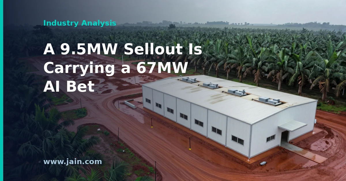
    Bitdeer’s 67MW Malaysia AI Bet Rests on a 9.5MW Sellout — and No Tenant Yet

    TL;DR · 30-second read

    The Short Version

    Bitdeer, a company best known for bitcoin mining, is adding a large computer center in Malaysia built for artificial intelligence work. It will draw about as much electricity as a sizable town and is due to be ready by mid-2027.

    The catch: no customer has signed up to rent it yet. Its main proof that people want this is a Malaysian site one-seventh the size, which sold out this summer.

    So it is a bet that customers will come, made while the company pays as much as 13% a year on some of its loans.

    Bitdeer Technologies (Nasdaq: BTDR), through its Bitdeer AI unit, has secured a 67MW AI data center campus in Malaysia, with delivery targeted for the second quarter of 2027, according to MarketScreener, StreetInsider and Crypto Briefing. TheEnergyMag reported that the addition brings Bitdeer’s total to 273.5MW. FourWeekMBA reported that no offtake has been signed. An offtake is a customer’s commitment to take the capacity. Investing.com put the facility at 60MW rather than 67MW. StreetInsider and Stocktwits reported that Bitdeer’s AI infrastructure pipeline tops $10 billion.

    Separately, Stock Titan reported that Bitdeer told readers to disregard a release that had cited a facility target of up to 350MW. MarketScreener reported that alerts on Bitdeer AI’s data center services agreement were withdrawn. The announcement follows a 6-K filed September 29, in which Bitdeer disclosed that its roughly 9.5MW A102 data center in Malaysia had sold out on five-year offtake commitments.

    Executive Summary

    Bitdeer is adding 67MW of AI data center capacity in Malaysia, a country where it already operates. Delivery is targeted for Q2 2027, only a few quarters away, and no customer has committed to the space. The only Malaysian AI contract the company has put on the record is the 9.5MW A102 sellout disclosed in its September 29 filing. The new campus is therefore about seven times larger than the demand Bitdeer has demonstrated in that market.

    The contrast with Bitdeer’s Norwegian project is sharp. At Tydal, the company signed a named tenant at a disclosed price before building, with roughly $1.3 billion of bank-arranged credit support behind the tenant. The Malaysian campus so far has a size and a date, but no tenant, price or financing disclosed. This is a speculative build, meaning one put up ahead of signed demand. It comes as Bitdeer carries collateralized loans at a 13.0% effective interest rate, with $373.5 million of principal falling due within a year of June 30, 2026.

    Two figure discrepancies need clearing up. One is the withdrawn reference to an up-to-350MW target. The other is the 60MW versus 67MW sizing. Until Bitdeer clarifies them, it is hard to say exactly what is being built.

    A 9.5MW Sellout Is the Demand Case for 67MW

    Bitdeer has put only one piece of Malaysian AI demand on the record, and it is small. In its September 29 6-K, the company said Bitdeer AI sold out approximately 9.5MW at its A102 data center in August, with five-year offtake commitments for its AI Cloud business, which sells computing capacity for AI workloads. The new campus, at 67MW, is about seven times that size. It is being added before any customer has committed to it.

    That ratio is the core of the bet. The A102 sellout shows that buyers in Malaysia will sign multi-year commitments for Bitdeer’s capacity. It does not show that buyers exist for seven times as much, on Bitdeer’s timeline and at the price it needs. The calendar is also short. Q2 2027 is two to three quarters away, so Bitdeer has quarters, not years, to sign tenants. If the campus is delivered before it is contracted, Bitdeer carries the cost of a finished facility with no revenue against it until the space fills.

    Different groups are affected in different ways. For AI companies looking for capacity in Southeast Asia, an uncommitted campus with a near-term delivery date gives them room to negotiate. For Bitdeer shareholders, the value of the project depends on when the first tenant signs and on what terms. A further question is how the space will be used. Bitdeer could fill the campus with its own AI Cloud service, as at A102, which means buying its own processors on top of the facility. Or it could lease the space as colocation, where the tenant brings its own hardware. Those two paths carry very different capital requirements.

    Tydal Is the Template Malaysia Has Not Yet Matched

    Bitdeer’s own filings show what a fully contracted AI campus looks like. Under the Tydal, Norway agreement with Volta Tydal AS, described in the September 29 6-K, Bitdeer’s subsidiary will deliver 121 IT MW of contracted critical load, supported by an estimated 133 gross MW. IT MW is the power available to the computers themselves. Gross MW also covers cooling and other building systems. The contract is worth approximately $4.7 billion over a 16-year base term, at an average rate of about $202 per kilowatt per month. Electricity is fully reimbursed by the tenant, and payments rise 3% a year. Bitdeer expects about $2.4 million of annual revenue per IT MW. It also expects a net operating income margin of roughly 90%, meaning the share of revenue left after operating the property.

    The tenant’s obligations are expected to be backed by letters of credit totaling about $1.3 billion, arranged by affiliates of J.P. Morgan and another major financial institution. These are bank guarantees that pay out if the tenant cannot. That backing is subject to customary conditions, and the tenant can terminate without a fee at year 10. So even Bitdeer’s strongest contract has conditions attached. Still, it has a named counterparty, a price, a term and credit support, all disclosed before construction completes. The design-and-construction contract for Tydal is phased to begin in December 2026.

    The Malaysian campus has none of those elements on the record yet. That is not unusual for a project announced early. But it means the 67MW should be read as capacity Bitdeer intends to sell, not capacity it has sold.

    13% Debt Puts a Clock on the Lease-Up

    Bitdeer’s balance sheet makes the timing of tenant signings more important. According to the financial statements filed September 29, the company’s collateralized loans from BIT Group carried a 13.0% effective interest rate in the first half of 2026. Interest expense on those loans was $32.7 million, up from $3.0 million a year earlier. As of June 30, $373.5 million of that principal was due within twelve months, and $142.1 million was due after that. The loans are secured by mining rigs, inventories and data center assets.

    Bitdeer has other obligations as well. It has a $26.0 million bank facility at 10.31% that matures in December 2026. It has $375.0 million of 5.00% convertible notes due 2032, issued in February. It also had roughly 3,669 Bitcoin outstanding under a separate BIT Group Bitcoin loan as of September 29. In August, the company paid about $100 million in cash for roughly 200 acres in Milam County, Texas. On October 8, its board authorized a new $100 million share buyback after fully using a previous $40 million program.

    None of that is unusual for a company expanding quickly. It does mean the Malaysian campus competes for capital with debt repayments, land acquisition and buybacks. Every quarter the campus sits unleased, capital stays committed with nothing coming back. Bitdeer has not said how the campus is being financed.

    One Figure Withdrawn, Another Disputed

    The withdrawn up-to-350MW reference is worth noting in a measured way. Companies correct releases for many reasons, and the figure that stands is the 67MW campus. But Bitdeer has not explained what the 350MW target referred to or whether a larger expansion is still under consideration. For a company that investors increasingly value on its pipeline of planned capacity, that clarification matters.

    The 60MW versus 67MW gap may have a simple explanation. The ratio is close to the IT-versus-gross distinction Bitdeer itself draws at Tydal, where 121 IT MW sits within 133 gross MW. But Bitdeer has not confirmed that this is the reason. It is a question the company can answer quickly. Buyers pricing capacity and investors modeling revenue need to know which number is the sellable one.

    Background

    Bitdeer Technologies Group is incorporated in the Cayman Islands, headquartered in Singapore and listed on the Nasdaq under the ticker BTDR. It built its business on bitcoin mining. Its revenue lines include self-mining, cloud hash rate (selling mining capacity to others), hosting and mining rig sales, plus a growing AI Cloud business. Its financial statements break out figures for Ethiopia, Canada, Malaysia, Norway, Bhutan, the United States and Singapore. The company cites about 3.0 GW of total power capacity across its global site portfolio.

    Like several miners, Bitdeer is repositioning its power-connected sites toward AI computing. In Norway, it is converting its Tydal data center into an AI facility, under a cost-plus construction contract phased to begin in December 2026. In Texas, it bought about 200 acres near its Rockdale facility in August for roughly $100 million in cash, giving it 742MW of existing and pipeline power capacity in Milam County. In Malaysia, its 9.5MW A102 site sold out to AI Cloud customers in August 2026.

    Sources

    Source: Bitdeer Technologies Expands Malaysian AI Data Center Capacity With 67MW Campus (MarketScreener): Bitdeer AI adds a 67MW Malaysian AI data center campus.

    Primary sources: Bitdeer 6-K filed October 8, 2026 (US$100 million share repurchase program); Bitdeer 6-K filed October 2, 2026 (resignation of director); Bitdeer 6-K filed September 29, 2026 (interim report); Exhibit 99.1 to 6-K filed September 29, 2026 (unaudited consolidated financial statements); Exhibit 99.2 to 6-K filed September 29, 2026 (recent developments).

    Further reporting: FourWeekMBA; StreetInsider; Stocktwits; TheEnergyMag; Crypto Briefing; MarketScreener (withdrawn alerts); Stock Titan; Investing.com.

  • AI’s Memory Squeeze Lifts ChipMOS 36.7% — and Its New Capacity Is Already Spoken For

    AI’s Memory Squeeze Lifts ChipMOS 36.7% — and Its New Capacity Is Already Spoken For

    TL;DR · 30-second read

    The Short Version

    A Taiwanese company that does the final steps of making memory chips just had its best three months ever. It wraps finished chips in protective casing and checks that they work. Sales were up about 37% from a year earlier.

    The reason is artificial intelligence. AI systems are using up memory chips faster than the world can make them. Memory chips are the parts that let a computer hold information while it works.

    The company is adding factory space, but says that space is already promised to existing customers. So there is little room left over for anyone else, even in the less famous steps of chipmaking.

    ChipMOS Technologies, a Taiwan-based provider of outsourced semiconductor assembly and test services (OSAT), reported record unaudited revenue of NT$8,400.8 million (US$263.8 million) for the third quarter of 2026 on October 8, 2026. That was up 13.8% from the second quarter and 36.7% from the third quarter of 2025. September revenue was NT$2,792.0 million (US$87.7 million), up 0.2% from August and 33.8% from September 2025.

    In a 6-K filed with the SEC the same day, the company attributed the growth to sustained AI-related demand outpacing available memory supply. It said new capacity from its continuing footprint expansion is being deployed to meet existing customer forecasts and long-term supply agreements.

    Executive Summary

    ChipMOS packages and tests chips, much of it memory. That is the back-end work that turns finished silicon into parts a server or phone maker can use. Its record quarter is the latest sign that AI demand is pulling on the whole memory supply chain, not only the companies that fabricate the chips.

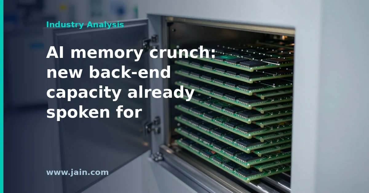
    The most consequential line in the release is not the 36.7% growth. It is the statement that new capacity is going to existing customer forecasts and long-term supply agreements, while structural supply constraints persist. In plain terms, the expansion ChipMOS is paying for has largely been claimed before it comes online. For hardware buyers, that means the back end of memory production offers little spare room in which a shortage could ease quickly.

    The company also said demand is broadening across most of its memory and storage end markets. That suggests AI’s pull on memory supply is spilling into conventional devices. The disclosure covers revenue only, however. Margins, pricing and the scale of the expansion are not yet public.

    New Capacity That Is Already Spoken For

    Chipmaking has two broad halves. The front end prints circuits onto silicon wafers. The back end cuts those wafers into individual chips, encases them in protective packages and tests each one before it ships. A memory chip that has been fabricated but not yet packaged and tested cannot go into a server. Back-end throughput is therefore as much a ceiling on usable supply as wafer output. ChipMOS sits in that back-end layer as an outsourced provider, serving fabless chip designers, integrated device manufacturers and foundries.

    ChipMOS says AI-related demand is outpacing available memory supply. It also says new capacity is being deployed to meet existing customer forecasts and long-term supply agreements. That combination is the operational signal. When a supplier says its expansion is already committed, the extra capacity does not show up as open slots that a new or occasional buyer can book. Customers with forecasts on file and contracts in place get the increment first. Everyone else competes for whatever remains.

    Memory makers’ customers feel this first. Downstream, so does anyone whose AI server or storage plans depend on memory arriving on schedule. ChipMOS describes the constraints as structural, not temporary. That language implies the company does not expect the imbalance to resolve within a quarter or two. It has not, however, said how long it expects the constraints to last.

    A Step Up in July, Then a Plateau

    The quarterly and monthly figures together show how the growth arrived. Third-quarter revenue of NT$8,400.8 million, minus August’s NT$2,785.7 million and September’s NT$2,792.0 million, implies July revenue of about NT$2,823.1 million. That makes July the strongest month of the three. August and September held almost exactly level, and September was up just 0.2% month on month.

    So the jump from the second quarter’s NT$7,383.1 million came as a step change at the start of the quarter, which then held at roughly NT$2.8 billion a month. Year-on-year growth stayed above 33% in both August and September. The higher level is sustained, but it did not keep climbing within the quarter. A flat run rate at a record level fits a business working through committed volume as fast as its lines allow. It could equally reflect order timing or product mix. ChipMOS has not said which.

    AI Demand Spilling Into Conventional Memory

    The release says demand is broadening across most of the company’s memory and storage end markets. That matters for understanding where AI’s pull ends up. When AI servers absorb a large share of available memory supply, buyers of memory for other products face tighter supply too. Back-end providers serving those markets then see demand from several directions at once. ChipMOS’s growth is consistent with that pattern, though the company has not broken out revenue by end market.

    The market has been paying attention. In a 6-K filed September 29, ChipMOS reported that trading in its securities had reached a Taiwan Stock Exchange disclosure threshold. Under exchange rules, that required the company to publish a notice pointing investors to its financial information.

    What the Revenue Figures Do and Do Not Establish

    Memory is historically one of the most cyclical corners of the semiconductor industry. The release’s mention of long-term supply agreements is relevant because such contracts can smooth volumes through a downturn. Without disclosed terms, though, their protective value is hard to judge. The company’s forward-looking statements also flag tariffs, trade-policy changes, exchange rates and recession risk as factors that could change results.

    The figures are unaudited consolidated revenue. All US-dollar amounts, including those for prior periods, are translated at a single September 30, 2026 rate of NT$31.85 to the dollar. The growth rates therefore reflect New Taiwan dollar performance, not currency movements. Revenue also says nothing on its own about profitability. A record top line built on constrained supply could carry strong margins. It could also carry elevated costs from the expansion under way. ChipMOS’s quarterly earnings report will show which.

    Background

    ChipMOS Technologies is headquartered in Hsinchu Science Park, Taiwan, and operates facilities in Hsinchu Science Park, Hsinchu Industrial Park and Southern Taiwan Science Park. It is dual-listed on the Taiwan Stock Exchange (8150) and Nasdaq (IMOS). It provides end-to-end assembly and test services to fabless chip designers, integrated device manufacturers and independent foundries across a wide range of end markets, with memory and storage a significant part of its business.

    Semiconductor production splits into front-end fabrication, where circuits are built on silicon wafers, and back-end assembly and test, where chips are separated, packaged and verified. Much of the attention on AI hardware has focused on leading-edge fabrication. But every chip, including the memory that AI servers consume in large quantities, must also pass through back-end lines before it can ship. That makes outsourced assembly and test providers an often-overlooked link in AI infrastructure supply.

    Sources

    Source: ChipMOS REPORTS RECORD HIGH QUARTERLY REVENUE; 33.8% YoY INCREASE IN SEPTEMBER 2026 REVENUE; 36.7% YoY INCREASE IN 3Q26 REVENUE, ChipMOS’s October 8, 2026 announcement of unaudited September and third-quarter revenue.

    Primary sources: ChipMOS Technologies Form 6-K filed October 8, 2026 (September 2026 and 3Q26 revenue); ChipMOS Technologies Form 6-K filed September 29, 2026 (TWSE trading-threshold financial disclosure).

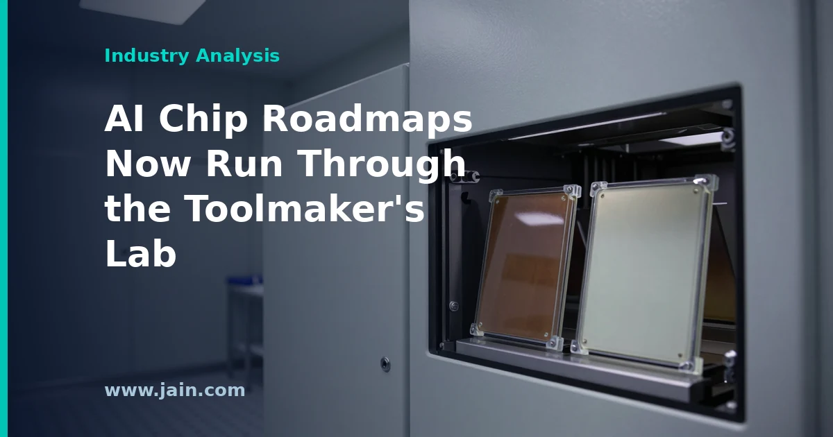
  • With Intel and TSMC in Applied’s $5B Lab, AI Chip Roadmaps Now Run Through a Toolmaker

    With Intel and TSMC in Applied’s $5B Lab, AI Chip Roadmaps Now Run Through a Toolmaker

    TL;DR · 30-second read

    The Short Version

    Intel, the American chipmaker, is expanding its research at a $5 billion lab in Silicon Valley run by Applied Materials, the company that builds the machines used to make computer chips.

    The twist: Intel’s biggest rival in making chips for other companies, Taiwan Semiconductor Manufacturing Company, signed on to the same lab earlier this year. Two fierce competitors will be inventing future chips under one roof.

    Why it matters: the chips behind artificial intelligence keep getting harder to make, and more of that early invention now happens at the machine maker, not inside any one chip company.

    shattered.io reported that Applied Materials and Intel announced on October 6, 2026 an expanded collaboration on next-generation transistors, interconnects and advanced packaging, centered on Applied’s EPIC Center in Silicon Valley and Intel’s research campus in Hillsboro, Oregon. The work explicitly includes Foveros, Intel’s technology for stacking chip components vertically.

    The EPIC Center, first pledged in May 2023 as an investment of up to $4 billion, is now described as a $5 billion facility. TSMC was confirmed as a founding partner in May 2026, five months before Intel’s expanded role was announced. No dollar figure, node target or performance goal was attached to the Intel agreement.

    Executive Summary

    Applied Materials, whose equipment sits inside virtually every leading-edge chip factory, now counts the two most closely watched advanced logic foundries (contract chip manufacturers) as research partners at the same facility. Intel’s expanded role covers the full stack of problems that limit AI processors: the transistors themselves, the microscopic wiring that connects them, and the packaging that joins multiple chip pieces into one product.

    Intel CEO Lip-Bu Tan tied the work directly to AI demand, citing the need for gains in performance, power efficiency and packaging, and described Applied as an important partner in moving new technology from the lab into high-volume manufacturing in the United States. Intel Foundry’s chief technology and operations officer, Naga Chandrasekaran, framed faster R&D as critical to keeping pace with AI infrastructure buildout.

    The significance lies less in any single deliverable, since none was disclosed, than in where the work is happening. When rival foundries both co-develop processes inside a toolmaker’s lab, the equipment vendor becomes a shared starting point for next-generation AI silicon.

    Why the Toolmaker’s Lab Is Becoming the Starting Line

    New chip generations do not begin at the factory. They begin with materials and process experiments: which film to deposit, how to etch a structure a few atoms wide, how to bond two pieces of silicon face to face. Those experiments depend on the equipment that will eventually run in production, which is why chipmakers co-develop processes with toolmakers. The EPIC Center, short for Equipment and Process Innovation and Commercialization, was built to formalize that step, with more than 180,000 square feet of cleanroom (ultra-clean manufacturing space) planned and up to 2,000 engineering jobs.

    The scope of the Intel work maps onto the three constraints that matter most for AI processors. Front-end-of-line research targets the transistor layer. Back-end-of-line research targets interconnects, the wiring stacked above the transistors, where electrical resistance grows as features shrink and can become a bigger limit on speed and power than the transistors themselves. Packaging research, including Intel’s Foveros 3D stacking of chiplets (smaller dies combined into one package), targets interconnect density, power delivery and heat, all of which limit how much compute can be packed into an AI accelerator.

    With TSMC as a founding partner and Intel as an expanded partner, at least part of the early-stage work on both companies’ next-generation AI silicon now passes through the same equipment vendor’s facility. That does not mean the two share designs or results; it means the toolmaker sees, and helps shape, both roadmaps. For AI chip designers who buy foundry capacity, it suggests that the process innovations available to them will increasingly be co-developed with Applied rather than invented in isolation inside one foundry.

    Intel’s Math: A $2.1 Billion Loss and a Need for Outside Customers

    Intel Foundry, the division that manufactures chips for Intel and outside customers, posted $5.8 billion in revenue and a $2.1 billion operating loss in its most recently reported quarter, a $348 million improvement on the prior period. Intel has raised its 2026 capital spending guidance to more than $20 billion company-wide, citing stronger customer-demand signals.

    The division’s path to profitability runs through external customers, and winning them requires showing that Intel’s advanced nodes and packaging can match TSMC on schedule and yield. Intel says its 18A process has been in volume production in Arizona since December. Moving from a node that works to a node that wins outside AI chip business is where materials and packaging co-development pays off, and packaging is one area where Intel has distinctive technology to offer.

    Neutral Ground Is Good Business for Applied

    For Applied Materials, hosting both foundries reduces dependence on any single customer’s spending cycle. The company reported fiscal third-quarter 2026 revenue of $9.12 billion, with $7.04 billion coming from its Semiconductor Systems segment, which sells the equipment used for leading-edge manufacturing. Every process co-developed at EPIC is, in practice, a process that runs on Applied tools.

    The facility’s cost has also grown: from a pledge of up to $4 billion over seven years in 2023 to a project now described as $5 billion. Cost growth is common in cleanroom-heavy construction, and anchor partners help justify it. The open question is how Applied manages confidentiality when two direct competitors work in the same building, a matter the companies have not addressed publicly.

    A Shared Lab Does Not Close the Spending Gap

    Shared research access can equalize the starting line for process experiments, but not manufacturing scale. TSMC has guided 2026 capital spending to $60 billion to $64 billion, up from roughly $56 billion, roughly three times Intel’s company-wide figure of more than $20 billion. Whoever converts lab results into high-volume production fastest still needs the factories to do it.

    Samsung Foundry, the third major advanced-logic contender, has no confirmed role at the EPIC Center, and its foundry results are reported inside Samsung Electronics’ broader semiconductor segment. For buyers of AI silicon, the practical takeaway is that process and packaging advances developed at EPIC may reach both Intel and TSMC customers, while capacity remains the differentiator.

    Background

    Applied Materials is one of the world’s largest makers of semiconductor manufacturing equipment, the deposition, etching and inspection machines that chip factories use to build transistors and wiring. It unveiled the EPIC Center in May 2023, pledging up to $4 billion in incremental investment over seven years, more than 180,000 square feet of cleanroom space, up to 2,000 engineering jobs and as many as 1,500 construction jobs. The project is now described as a $5 billion facility and is scheduled to be operationally ready in 2026.

    Intel Foundry is Intel’s contract-manufacturing division, built to produce chips for outside customers as well as Intel’s own products, in direct competition with TSMC, the world’s largest contract chipmaker. Intel CEO Lip-Bu Tan has positioned AI demand and US-based high-volume manufacturing as central to the foundry strategy.

    Sources

    Source: Intel Joins TSMC at Applied Materials’ $5B Chip Lab [2026] (shattered.io), covering Intel’s expanded R&D collaboration with Applied Materials at the EPIC Center, where TSMC is a founding partner.

  • Applied Digital’s $1.59B at 7% Ties Its AI Campus Debt to Go-Live Speed

    Applied Digital’s $1.59B at 7% Ties Its AI Campus Debt to Go-Live Speed

    TL;DR · 30-second read

    The Short Version

    Applied Digital builds huge buildings packed with computers that tech giants rent to run artificial intelligence. Its sales more than quadrupled from a year earlier, to $341.9 million in three months.

    It still lost $221 million under standard accounting rules. It also borrowed $1.59 billion at 7% interest, about $111 million a year, to build another one.

    The catch: interest is owed from the day the money is borrowed, but rent only starts once a building is finished and a tenant moves in. How fast that gap closes is the thing to watch.

    Applied Digital (Nasdaq: APLD) reported results on October 7, 2026 for its fiscal first quarter of 2027, the three months ended August 31. Revenue was $341.9 million, up 322% from a year earlier. The net loss attributable to common stockholders was $221.0 million, or $0.76 per share. On the company’s adjusted basis, which excludes its majority-owned ChronoScale subsidiary, the loss narrowed to $4.1 million, or $0.01 per share, and adjusted EBITDA (earnings before interest, taxes, depreciation and amortization) was $64.4 million.

    The company said its Polaris Forge 1 campus in North Dakota reached 250 megawatts (MW) of live capacity on October 1. During the quarter it closed $1.59 billion of 7.000% senior secured notes due 2031 to fund a third 150 MW building there and repay a $300 million bridge loan. Barron’s read the results as a sign the company’s data center bet is starting to pay off.

    Executive Summary

    The quarter marks Applied Digital’s transition from a company announcing capacity to one reporting what that capacity earns. Live capacity at Polaris Forge 1 went from 100 MW to 175 MW on July 1 and to 250 MW on October 1. The company expects initial operations at Polaris Forge 2 in Harwood, North Dakota, to bring total delivered critical IT load across its North Dakota campuses to 300 MW by the end of calendar 2026. Critical IT load is the power available to the computing equipment itself, not counting cooling and other building systems.

    The financing came at the same pace. The $1.59 billion note issue, made through subsidiary APLD ComputeCo 3 LLC, adds a fixed interest bill that starts before the building it funds produces any rent. The 210 MW, 15-year lease at Delta Forge 2, which the company valued at about $5.2 billion of base-term contracted revenue, shows the scale of the revenue on offer. The question for the next several quarters is how quickly finished halls convert into recognized lease revenue. This quarter’s results only partly answer it, because the newest 75 MW came online after the period closed.

    Why Go-Live Speed Now Sets the Debt Math

    The $1.59 billion of 7.000% senior secured notes, issued at par and listed among the quarter’s highlights, carry about $111.3 million of interest a year. That works out to roughly $27.8 million a quarter, or about $9.3 million a month, on these notes alone. The proceeds pay for construction of a third, 150 MW high-performance computing building at Polaris Forge 1 and repay a $300 million bridge loan. Simple subtraction leaves roughly $1.29 billion for construction before fees. Interest accrues from the day the notes are issued. The building earns nothing until it is delivered and its lease begins.

    That gap is the mechanism behind this article’s headline. Every month between closing and lease commencement on building three is a month of coupon payments with no matching rent from the asset that secures the debt. Because the notes were issued through a project-level subsidiary, APLD ComputeCo 3 LLC, lenders are underwriting that specific building’s timeline. For a sense of how much revenue rides on timing, the company’s Delta Forge 2 lease implies about $1.65 million per megawatt per year in average base-term revenue ($5.2 billion over 15 years across 210 MW). Applied Digital has not said whether building three is priced similarly.

    The people affected go beyond shareholders. Noteholders depend on the construction schedule. Contractors and equipment suppliers carry the schedule risk. Tenants need the halls ready when their own chip deliveries arrive. Applied Digital’s track record helps here. It hit two 75 MW Ready for Service milestones, on July 1 and October 1, roughly a quarter apart. Ready for Service is the point at which a finished, powered data hall is handed over for use. The company’s next proof point is whether building three follows a similar cadence.

    322% Growth and a $221 Million Loss Describe the Same Quarter

    Barron’s take that the bet is starting to pay off holds on the company’s operating measures. Adjusted EBITDA was $64.4 million, and net operating income was $58.8 million. Net operating income is a real-estate-style measure of property-level income before corporate overhead and financing costs. On the adjusted basis the company was close to break-even, with a $4.1 million loss.

    Under standard accounting (GAAP), the loss attributable to common stockholders was $221.0 million. The roughly $217 million gap between that figure and the adjusted loss is large for a single quarter. Investors will want to examine the company’s reconciliation of the two closely. Part of the gap reflects the exclusion of ChronoScale, Applied Digital’s majority-owned, separately listed accelerated-compute business, which is consolidated in GAAP results but stripped out of the adjusted figures. The 10-Q filed the same day also shows Series E, E-1 and G preferred stock in the capital structure. That matters because any preferred dividends sit ahead of common holders, and the headline loss is measured after them.

    Neither reading is wrong. They answer different questions. The adjusted figures show what the operating data center business is starting to generate. The GAAP figure shows what the whole enterprise, including its financing and its subsidiary, cost shareholders this quarter.

    The Reported Quarter Mostly Predates the Capacity That Matters

    The timing explains why this is only the first part of the test. In the quarter ended August 31, Polaris Forge 1 ran at about 100 MW for June and 175 MW for July and August. The second 75 MW phase of Building 2 did not reach Ready for Service until October 1, a month after the quarter closed. Fiscal Q2, which runs September through November, will include one month at 175 MW and two at 250 MW. Fiscal Q3 is the first quarter that could reflect the full 250 MW. If Polaris Forge 2 starts on schedule, that quarter would also include the start of Harwood.

    Applied Digital has not broken out how much of its $300.4 million in adjusted revenue came from Polaris Forge 1. It also has not said whether the October 1 phase began billing on its Ready for Service date. Revenue per live megawatt, tracked quarter to quarter, is the clearest test of whether delivered capacity is turning into recognized revenue on schedule. Two more quarters of data should make that measurable.

    Power Is Being Secured Ahead of Buildings

    After the quarter, Applied Digital signed a power purchase agreement with Base Electron for capacity and energy from an approximately 1,200 MW natural gas-fired plant that Base Electron is to develop in North Dakota. It also agreed to up to approximately 1 GW of potential power capacity in Finland. Both are long-dated options on future growth, not operating capacity. In the case of Base Electron, the plant has not yet been built.

    This sequencing reflects a real constraint. Grid power is now one of the slowest inputs to an AI campus, and the company argues that low-cost, power-rich regions will hold value better as coastal and metro markets tighten. Chief Executive Wes Cummins framed the strategy around “durable, high-quality, long-term contracts” with investment-grade hyperscalers, meaning the largest cloud and AI platform operators. Securing power ahead of signed tenants creates an obligation to fill that capacity. Each new campus will also need its own financing, likely structured like the ComputeCo 3 notes. The Delta Forge 2 lease shows hyperscaler demand exists. Matching that demand to each new block of power is the ongoing execution test.

    Background

    Applied Digital is a Dallas-based company that designs, builds, owns and operates large data centers purpose-built for high-performance computing, including artificial intelligence training and inference. Its strategy centers on North Dakota, where it operates Polaris Forge 1 and is developing Polaris Forge 2 in Harwood and Polaris Forge 3 in Oliver County. Its stated goal is to lease capacity on long-term contracts to investment-grade hyperscalers, the largest cloud and AI platform operators.

    The company also holds a majority stake in ChronoScale, a separately listed company that runs its legacy cloud services business and is pursuing a 50 MW deployment with Microsoft built on NVIDIA GB300 NVL72 rack-scale systems with liquid cooling. Because ChronoScale is consolidated, Applied Digital reports both GAAP figures and adjusted figures that exclude it. Investing.com’s market wrap placed the results alongside a broader wave of AI-related debt deals, which is the financing context for this buildout.

    Sources

    Source: Applied Digital’s Earnings Show Its Data Center Bet Is Starting to Pay Off (Barron’s), on Applied Digital’s fiscal first-quarter 2027 results; and AI debt deal wave reports; Applied Digital reports – what’s moving markets (Investing.com), a market wrap covering the results.

    Primary sources: Applied Digital Form 10-Q for the quarter ended August 31, 2026 (filed October 7, 2026); Applied Digital Form 8-K (filed October 7, 2026); Applied Digital Reports Fiscal First Quarter 2027 Results (Exhibit 99.1 to 8-K).

  • TSMC’s 54.6% September Surge Moves AI’s Next Test to Power and Data Center Sites

    TSMC’s 54.6% September Surge Moves AI’s Next Test to Power and Data Center Sites

    TL;DR · 30-second read

    The Short Version

    TSMC, the Taiwanese company that manufactures chips designed by many of the best-known technology firms, said its September sales were 54.6 percent higher than a year earlier. That is more than one and a half times last year’s level.

    News reports tie the jump to demand for chips that run artificial intelligence tools such as chatbots.

    Why it matters: every one of those chips eventually needs a building, electricity and cooling before it can do any work. Chip supply is clearly growing fast. More of the challenge now falls on the power lines and buildings that have to house it.

    Taiwan Semiconductor Manufacturing Company (TSMC) reported consolidated revenue of approximately NT$511.86 billion for September 2026, in a Form 6-K filed with the US Securities and Exchange Commission on October 8. That figure was 54.6% higher than September 2025 and 0.6% lower than August 2026. Revenue for January through September totalled NT$3,898.73 billion, up 41.1% from the same period of 2025.

    CNBC and Anadolu Agency attributed the growth to demand for AI chips. Yahoo Finance Canada reported that TSMC’s third-quarter sales beat analysts’ estimates.

    Executive Summary

    The world’s largest contract chipmaker ended the third quarter at a monthly revenue level more than half again above a year earlier. September’s 54.6% year-on-year gain also outpaced the company’s 41.1% growth for the first nine months. In plain terms, growth did not fade as the year went on. Later months grew faster than earlier ones.

    The month-on-month figure matters too. September came in just 0.6% below August, so TSMC is holding revenue at an elevated plateau rather than posting a one-off spike. For the AI infrastructure supply chain, that means a sustained and growing stream of advanced silicon leaving the fab. Every piece of it has to be packaged, built into servers, and installed in a powered, cooled data hall before it produces any computing.

    That is the operational point of this report. When the most important upstream supplier keeps scaling at this pace, the question of whether there will be enough AI capacity depends increasingly on the steps after the wafer: advanced packaging, grid connections, electrical equipment, cooling and construction-ready sites.

    A Plateau at a Record Height

    The headline 54.6% is a year-on-year comparison. The more telling numbers sit alongside it. Divide the nine-month total of NT$3,898.73 billion by nine and the average month comes to roughly NT$433 billion. September’s NT$511.86 billion ran well above that. The 54.6% September growth rate also exceeds the 41.1% year-to-date rate, which means the back half of the period is pulling the average up. This is acceleration, not a business coasting on early-year strength.

    The 0.6% dip from August is small enough to read as noise. Monthly foundry revenue moves with shipment timing, and TSMC’s filing gives no reason for the change. What the two adjacent months show together is a run rate holding near its peak. For customers waiting on allocation, that matters more than any single month’s swing.

    Two caveats apply. Revenue is not the same as units: higher prices for leading-edge processes and a richer product mix can lift sales faster than wafer volumes. The figures are also reported in New Taiwan dollars, so growth measured in US dollars can differ with exchange-rate movements.

    Why the Pressure Moves Past the Fab

    A finished wafer is not AI capacity. The chips cut from it must be joined with high-bandwidth memory in advanced packaging, where several chips are bonded together into a single module. TSMC performs a large share of this work for leading accelerators. The modules then go into servers and racks. Those racks need a building with enough electrical capacity, transformers and switchgear, plus cooling that can handle far denser heat loads than conventional servers produce. Foundry revenue is the earliest measurable point in that chain, which is why a sustained 54.6% rise at the dominant supplier is a leading signal for everyone downstream.

    The lead times diverge sharply. A foundry can raise output on existing lines within months. A new utility grid connection, a high-voltage substation or a permitted greenfield campus often takes years. When the upstream stage scales at this pace and holds there, the steps that cannot speed up become the ones that set the pace. Those are packaging lines, power delivery and shovel-ready land. That is the sense in which the next test for AI capacity moves past the fab.

    Those most affected are colocation and wholesale data center developers competing for powered land, utilities fielding large-load requests, makers of transformers and cooling equipment, and the cloud providers who have bought chips they now need to energise. One fair counterpoint: a flat month-on-month revenue line could also mean TSMC itself is running close to its own capacity ceiling. The data supports “growing fast and sustained.” It does not prove that the foundry has stopped being a constraint.

    The Overseas Buildout Is in the Footnotes

    The same 6-K reports intercompany financing that shows where TSMC is putting its balance sheet. It records funds lent to TSMC Washington and guarantees provided to TSMC Arizona, TSMC North America and TSMC Global, all wholly owned subsidiaries. It also lists derivative positions at TSMC China, TSMC Nanjing and Japan Advanced Semiconductor Manufacturing, the company’s Japanese manufacturing affiliate.

    None of this is new strategy, but it does underline how the parent is backing overseas manufacturing. For US data center buyers, Arizona production is relevant to supply resilience and to customers who want domestically fabricated chips. Revenue strength at the parent level makes that support easier to sustain. The filing, however, does not link these arrangements to specific capacity additions or dates.

    What the Beat Does and Does Not Prove

    A third-quarter beat confirms that demand ran ahead of what analysts had modelled. It does not show how much of that demand is AI accelerators rather than smartphones, PCs or other products, because the monthly report has no breakdown by technology or customer. Margins, capital spending and guidance will come with TSMC’s full quarterly results.

    For infrastructure planners, the practical reading is cautious but clear. Chip supply is not the stage showing strain in this data. Operators who assume silicon will be the gating item for 2027 deployments may find the gating item is instead an energised building.

    Background

    Taiwan Semiconductor Manufacturing Company, headquartered in Hsinchu Science Park and listed in Taipei (2330) and New York (TSM), pioneered the pure-play foundry model: it manufactures chips designed by other companies rather than selling its own. That model has made it the central manufacturer for most leading-edge processors, including the accelerators used to train and run AI models.

    TSMC publishes revenue monthly, which makes it one of the earliest public indicators of semiconductor demand. Full quarterly results follow with margins and guidance. In recent years the company has expanded beyond Taiwan with operations in Arizona and Washington state, China, and Japan through its Japan Advanced Semiconductor Manufacturing affiliate.

    Sources

    Source: TSMC September revenue jumps 54.6% as AI chip demand fuels growth (Anadolu Ajansı), a report on TSMC’s September 2026 revenue. Related coverage: TSMC’s September sales surge year-over-year as AI drives chip demand (CNBC); TSMC Q3 sales beat estimates on surging AI chip demand (Yahoo! Finance Canada).

    Primary sources: Taiwan Semiconductor Manufacturing Company, Form 6-K: TSMC September 2026 Revenue Report, filed October 8, 2026 (SEC EDGAR).

  • A $40B Loan for Nvidia Chips Would Make SpaceX’s AI Buildout a Credit Story

    A $40B Loan for Nvidia Chips Would Make SpaceX’s AI Buildout a Credit Story

    TL;DR · 30-second read

    The Short Version

    SpaceX, the rocket and satellite company, is reportedly negotiating to borrow $40 billion to buy computer chips from Nvidia, the company whose chips run most artificial intelligence tools.

    Apollo, a giant investment firm, would lead the lending, so the chips would be bought with borrowed money rather than money SpaceX already has.

    Why it matters: when buying chips depends on loans this large, the AI boom also depends on lenders getting repaid, and AI chips lose value quickly as newer ones arrive.

    SpaceX is in talks to borrow $40 billion to buy Nvidia chips, Bloomberg reported. The Financial Times, in a report relayed by Reuters, said Apollo Global Management is leading the financing. No signed agreement has been announced. SpaceX and Apollo have not disclosed terms, the chip quantities, or a timeline.

    Executive Summary

    The reported financing would put a $40 billion debt package, led by one of the largest private-credit managers, behind a single company’s purchase of AI chips. Private credit means loans made by investment firms rather than banks. Nvidia’s graphics processing units (GPUs) are the specialised processors that train and run most large AI models, and they are the most expensive line item in an AI data center.

    It matters because of how the purchase is paid for, not only because of its size. A buyer that pays for chips from operating cash or new equity bears the risk itself. A buyer that borrows $40 billion takes on fixed repayment obligations, and its lenders take on part of the risk. If the talks conclude, how fast SpaceX adds AI computing capacity would depend partly on lender terms, collateral and repayment schedules.

    Why a $40 Billion Loan Turns Compute Into a Credit Question

    A company that buys AI chips with its own cash answers mainly to its shareholders. If the chips earn less than expected, the owners absorb the loss. A company that borrows $40 billion for the same purchase faces a different test. Interest and principal fall due on a schedule whether or not the hardware is fully used. The lenders, here a group led by Apollo, have to decide in advance how much the chips will earn and how quickly that cash will come in.

    That changes the questions that decide the deal. Before committing, lenders typically ask what revenue the computing capacity will produce, how quickly the chips lose value, what they could recover if repayment faltered, and how long the loan runs compared with the hardware’s useful life. None of the terms have been made public. Still, at $40 billion, the answers to those questions would shape the pace and cost of SpaceX’s chip purchases as much as Nvidia’s supply would.

    Several groups are exposed. SpaceX would take on fixed obligations. Apollo and any co-lenders, along with the investors whose money they deploy, would take on part of the hardware risk. Nvidia would book demand that rests partly on borrowed money rather than the buyer’s own funds.

    Why a Private-Credit Manager Would Lead

    Private-credit firms raise long-term capital from insurers, pension funds and other institutions. They can commit large sums to a single borrower and set terms privately, without the public pricing of a bond sale. That makes them a natural fit for a borrower seeking a very large, bespoke package. Reports describe Apollo as leading the financing, which suggests other lenders could take part, though no participants have been named.

    Apollo’s balance sheet shows why insurance-linked capital matters to firms like it. In an 8-K filed October 5, Apollo said Athene, its retirement-services subsidiary, holds most of its alternative investments, and estimated third-quarter alternative net investment income of about $375 million pre-tax, an annualised return of roughly 10%. That filing previews quarterly results and does not mention SpaceX or Nvidia. Whether any of the SpaceX exposure would end up on Athene’s books has not been disclosed.

    The Depreciation Problem Lenders Have to Price

    AI chips lose value faster than most assets usually financed with long-term debt. Nvidia releases new GPU generations frequently, and each one cuts the market value of the last. A loan secured against chips, or repaid from the revenue they generate, is only as sound as its assumptions about how long the hardware stays competitive.

    Lenders in AI financings have used the chips themselves as collateral (security that a lender can seize if a loan is not repaid). SpaceX and Apollo have not said whether this deal would be secured that way, or backed instead by SpaceX’s broader business. The difference matters. A loan backed by GPUs ties the lender’s recovery to second-hand chip prices. A loan backed by the whole company ties it to SpaceX’s overall cash flow.

    What Follows Downstream: Sites, Power and Cooling

    Chips bought with $40 billion of debt only start earning once they are installed and running, so delays in data center capacity become delays in repaying the loan. Each rack of high-end GPUs needs floor space, a reliable electricity supply and, increasingly, liquid cooling, because air alone cannot remove the heat dense AI hardware produces.

    For data center developers, utilities and cooling suppliers, debt-financed purchases make the timetable less forgiving. Hardware that sits in a warehouse waiting for power still accrues interest. SpaceX has not disclosed where the chips would be deployed or how much electrical capacity they would require.

    Background

    Nvidia’s GPUs, originally built for graphics, became the default hardware for training and running large AI models. They are now the most expensive single component of an AI data center, and buyers have funded them through operating cash, equity and, increasingly, debt. SpaceX is best known for rocket launches and satellite services.

    Apollo Global Management is a New York-based alternative asset manager. Its businesses include private credit and retirement services through its subsidiary Athene. Apollo is scheduled to report third-quarter results on November 3, 2026, according to its October 5 SEC filing.

    Sources

    Source: SpaceX in Talks to Borrow $40 Billion to Buy Nvidia Chips (Bloomberg), reporting SpaceX’s talks to borrow $40 billion for Nvidia chips; see also SpaceX seeks $40 billion financing led by Apollo to buy Nvidia chips, FT reports (Reuters).

    Primary sources: Apollo Global Management Form 8-K, filed October 5, 2026 (preliminary third-quarter alternative net investment income).