Author: Deepak Jain

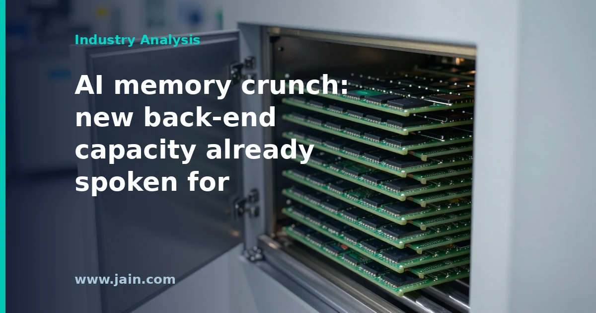
  • AI’s Memory Squeeze Lifts ChipMOS 36.7% — and Its New Capacity Is Already Spoken For

    AI’s Memory Squeeze Lifts ChipMOS 36.7% — and Its New Capacity Is Already Spoken For

    TL;DR · 30-second read

    The Short Version

    A Taiwanese company that does the final steps of making memory chips just had its best three months ever. It wraps finished chips in protective casing and checks that they work. Sales were up about 37% from a year earlier.

    The reason is artificial intelligence. AI systems are using up memory chips faster than the world can make them. Memory chips are the parts that let a computer hold information while it works.

    The company is adding factory space, but says that space is already promised to existing customers. So there is little room left over for anyone else, even in the less famous steps of chipmaking.

    ChipMOS Technologies, a Taiwan-based provider of outsourced semiconductor assembly and test services (OSAT), reported record unaudited revenue of NT$8,400.8 million (US$263.8 million) for the third quarter of 2026 on October 8, 2026. That was up 13.8% from the second quarter and 36.7% from the third quarter of 2025. September revenue was NT$2,792.0 million (US$87.7 million), up 0.2% from August and 33.8% from September 2025.

    In a 6-K filed with the SEC the same day, the company attributed the growth to sustained AI-related demand outpacing available memory supply. It said new capacity from its continuing footprint expansion is being deployed to meet existing customer forecasts and long-term supply agreements.

    Executive Summary

    ChipMOS packages and tests chips, much of it memory. That is the back-end work that turns finished silicon into parts a server or phone maker can use. Its record quarter is the latest sign that AI demand is pulling on the whole memory supply chain, not only the companies that fabricate the chips.

    The most consequential line in the release is not the 36.7% growth. It is the statement that new capacity is going to existing customer forecasts and long-term supply agreements, while structural supply constraints persist. In plain terms, the expansion ChipMOS is paying for has largely been claimed before it comes online. For hardware buyers, that means the back end of memory production offers little spare room in which a shortage could ease quickly.

    The company also said demand is broadening across most of its memory and storage end markets. That suggests AI’s pull on memory supply is spilling into conventional devices. The disclosure covers revenue only, however. Margins, pricing and the scale of the expansion are not yet public.

    New Capacity That Is Already Spoken For

    Chipmaking has two broad halves. The front end prints circuits onto silicon wafers. The back end cuts those wafers into individual chips, encases them in protective packages and tests each one before it ships. A memory chip that has been fabricated but not yet packaged and tested cannot go into a server. Back-end throughput is therefore as much a ceiling on usable supply as wafer output. ChipMOS sits in that back-end layer as an outsourced provider, serving fabless chip designers, integrated device manufacturers and foundries.

    ChipMOS says AI-related demand is outpacing available memory supply. It also says new capacity is being deployed to meet existing customer forecasts and long-term supply agreements. That combination is the operational signal. When a supplier says its expansion is already committed, the extra capacity does not show up as open slots that a new or occasional buyer can book. Customers with forecasts on file and contracts in place get the increment first. Everyone else competes for whatever remains.

    Memory makers’ customers feel this first. Downstream, so does anyone whose AI server or storage plans depend on memory arriving on schedule. ChipMOS describes the constraints as structural, not temporary. That language implies the company does not expect the imbalance to resolve within a quarter or two. It has not, however, said how long it expects the constraints to last.

    A Step Up in July, Then a Plateau

    The quarterly and monthly figures together show how the growth arrived. Third-quarter revenue of NT$8,400.8 million, minus August’s NT$2,785.7 million and September’s NT$2,792.0 million, implies July revenue of about NT$2,823.1 million. That makes July the strongest month of the three. August and September held almost exactly level, and September was up just 0.2% month on month.

    So the jump from the second quarter’s NT$7,383.1 million came as a step change at the start of the quarter, which then held at roughly NT$2.8 billion a month. Year-on-year growth stayed above 33% in both August and September. The higher level is sustained, but it did not keep climbing within the quarter. A flat run rate at a record level fits a business working through committed volume as fast as its lines allow. It could equally reflect order timing or product mix. ChipMOS has not said which.

    AI Demand Spilling Into Conventional Memory

    The release says demand is broadening across most of the company’s memory and storage end markets. That matters for understanding where AI’s pull ends up. When AI servers absorb a large share of available memory supply, buyers of memory for other products face tighter supply too. Back-end providers serving those markets then see demand from several directions at once. ChipMOS’s growth is consistent with that pattern, though the company has not broken out revenue by end market.

    The market has been paying attention. In a 6-K filed September 29, ChipMOS reported that trading in its securities had reached a Taiwan Stock Exchange disclosure threshold. Under exchange rules, that required the company to publish a notice pointing investors to its financial information.

    What the Revenue Figures Do and Do Not Establish

    Memory is historically one of the most cyclical corners of the semiconductor industry. The release’s mention of long-term supply agreements is relevant because such contracts can smooth volumes through a downturn. Without disclosed terms, though, their protective value is hard to judge. The company’s forward-looking statements also flag tariffs, trade-policy changes, exchange rates and recession risk as factors that could change results.

    The figures are unaudited consolidated revenue. All US-dollar amounts, including those for prior periods, are translated at a single September 30, 2026 rate of NT$31.85 to the dollar. The growth rates therefore reflect New Taiwan dollar performance, not currency movements. Revenue also says nothing on its own about profitability. A record top line built on constrained supply could carry strong margins. It could also carry elevated costs from the expansion under way. ChipMOS’s quarterly earnings report will show which.

    Background

    ChipMOS Technologies is headquartered in Hsinchu Science Park, Taiwan, and operates facilities in Hsinchu Science Park, Hsinchu Industrial Park and Southern Taiwan Science Park. It is dual-listed on the Taiwan Stock Exchange (8150) and Nasdaq (IMOS). It provides end-to-end assembly and test services to fabless chip designers, integrated device manufacturers and independent foundries across a wide range of end markets, with memory and storage a significant part of its business.

    Semiconductor production splits into front-end fabrication, where circuits are built on silicon wafers, and back-end assembly and test, where chips are separated, packaged and verified. Much of the attention on AI hardware has focused on leading-edge fabrication. But every chip, including the memory that AI servers consume in large quantities, must also pass through back-end lines before it can ship. That makes outsourced assembly and test providers an often-overlooked link in AI infrastructure supply.

    Sources

    Source: ChipMOS REPORTS RECORD HIGH QUARTERLY REVENUE; 33.8% YoY INCREASE IN SEPTEMBER 2026 REVENUE; 36.7% YoY INCREASE IN 3Q26 REVENUE, ChipMOS’s October 8, 2026 announcement of unaudited September and third-quarter revenue.

    Primary sources: ChipMOS Technologies Form 6-K filed October 8, 2026 (September 2026 and 3Q26 revenue); ChipMOS Technologies Form 6-K filed September 29, 2026 (TWSE trading-threshold financial disclosure).

  • With Intel and TSMC in Applied’s $5B Lab, AI Chip Roadmaps Now Run Through a Toolmaker

    With Intel and TSMC in Applied’s $5B Lab, AI Chip Roadmaps Now Run Through a Toolmaker

    TL;DR · 30-second read

    The Short Version

    Intel, the American chipmaker, is expanding its research at a $5 billion lab in Silicon Valley run by Applied Materials, the company that builds the machines used to make computer chips.

    The twist: Intel’s biggest rival in making chips for other companies, Taiwan Semiconductor Manufacturing Company, signed on to the same lab earlier this year. Two fierce competitors will be inventing future chips under one roof.

    Why it matters: the chips behind artificial intelligence keep getting harder to make, and more of that early invention now happens at the machine maker, not inside any one chip company.

    shattered.io reported that Applied Materials and Intel announced on October 6, 2026 an expanded collaboration on next-generation transistors, interconnects and advanced packaging, centered on Applied’s EPIC Center in Silicon Valley and Intel’s research campus in Hillsboro, Oregon. The work explicitly includes Foveros, Intel’s technology for stacking chip components vertically.

    The EPIC Center, first pledged in May 2023 as an investment of up to $4 billion, is now described as a $5 billion facility. TSMC was confirmed as a founding partner in May 2026, five months before Intel’s expanded role was announced. No dollar figure, node target or performance goal was attached to the Intel agreement.

    Executive Summary

    Applied Materials, whose equipment sits inside virtually every leading-edge chip factory, now counts the two most closely watched advanced logic foundries (contract chip manufacturers) as research partners at the same facility. Intel’s expanded role covers the full stack of problems that limit AI processors: the transistors themselves, the microscopic wiring that connects them, and the packaging that joins multiple chip pieces into one product.

    Intel CEO Lip-Bu Tan tied the work directly to AI demand, citing the need for gains in performance, power efficiency and packaging, and described Applied as an important partner in moving new technology from the lab into high-volume manufacturing in the United States. Intel Foundry’s chief technology and operations officer, Naga Chandrasekaran, framed faster R&D as critical to keeping pace with AI infrastructure buildout.

    The significance lies less in any single deliverable, since none was disclosed, than in where the work is happening. When rival foundries both co-develop processes inside a toolmaker’s lab, the equipment vendor becomes a shared starting point for next-generation AI silicon.

    Why the Toolmaker’s Lab Is Becoming the Starting Line

    New chip generations do not begin at the factory. They begin with materials and process experiments: which film to deposit, how to etch a structure a few atoms wide, how to bond two pieces of silicon face to face. Those experiments depend on the equipment that will eventually run in production, which is why chipmakers co-develop processes with toolmakers. The EPIC Center, short for Equipment and Process Innovation and Commercialization, was built to formalize that step, with more than 180,000 square feet of cleanroom (ultra-clean manufacturing space) planned and up to 2,000 engineering jobs.

    The scope of the Intel work maps onto the three constraints that matter most for AI processors. Front-end-of-line research targets the transistor layer. Back-end-of-line research targets interconnects, the wiring stacked above the transistors, where electrical resistance grows as features shrink and can become a bigger limit on speed and power than the transistors themselves. Packaging research, including Intel’s Foveros 3D stacking of chiplets (smaller dies combined into one package), targets interconnect density, power delivery and heat, all of which limit how much compute can be packed into an AI accelerator.

    With TSMC as a founding partner and Intel as an expanded partner, at least part of the early-stage work on both companies’ next-generation AI silicon now passes through the same equipment vendor’s facility. That does not mean the two share designs or results; it means the toolmaker sees, and helps shape, both roadmaps. For AI chip designers who buy foundry capacity, it suggests that the process innovations available to them will increasingly be co-developed with Applied rather than invented in isolation inside one foundry.

    Intel’s Math: A $2.1 Billion Loss and a Need for Outside Customers

    Intel Foundry, the division that manufactures chips for Intel and outside customers, posted $5.8 billion in revenue and a $2.1 billion operating loss in its most recently reported quarter, a $348 million improvement on the prior period. Intel has raised its 2026 capital spending guidance to more than $20 billion company-wide, citing stronger customer-demand signals.

    The division’s path to profitability runs through external customers, and winning them requires showing that Intel’s advanced nodes and packaging can match TSMC on schedule and yield. Intel says its 18A process has been in volume production in Arizona since December. Moving from a node that works to a node that wins outside AI chip business is where materials and packaging co-development pays off, and packaging is one area where Intel has distinctive technology to offer.

    Neutral Ground Is Good Business for Applied

    For Applied Materials, hosting both foundries reduces dependence on any single customer’s spending cycle. The company reported fiscal third-quarter 2026 revenue of $9.12 billion, with $7.04 billion coming from its Semiconductor Systems segment, which sells the equipment used for leading-edge manufacturing. Every process co-developed at EPIC is, in practice, a process that runs on Applied tools.

    The facility’s cost has also grown: from a pledge of up to $4 billion over seven years in 2023 to a project now described as $5 billion. Cost growth is common in cleanroom-heavy construction, and anchor partners help justify it. The open question is how Applied manages confidentiality when two direct competitors work in the same building, a matter the companies have not addressed publicly.

    A Shared Lab Does Not Close the Spending Gap

    Shared research access can equalize the starting line for process experiments, but not manufacturing scale. TSMC has guided 2026 capital spending to $60 billion to $64 billion, up from roughly $56 billion, roughly three times Intel’s company-wide figure of more than $20 billion. Whoever converts lab results into high-volume production fastest still needs the factories to do it.

    Samsung Foundry, the third major advanced-logic contender, has no confirmed role at the EPIC Center, and its foundry results are reported inside Samsung Electronics’ broader semiconductor segment. For buyers of AI silicon, the practical takeaway is that process and packaging advances developed at EPIC may reach both Intel and TSMC customers, while capacity remains the differentiator.

    Background

    Applied Materials is one of the world’s largest makers of semiconductor manufacturing equipment, the deposition, etching and inspection machines that chip factories use to build transistors and wiring. It unveiled the EPIC Center in May 2023, pledging up to $4 billion in incremental investment over seven years, more than 180,000 square feet of cleanroom space, up to 2,000 engineering jobs and as many as 1,500 construction jobs. The project is now described as a $5 billion facility and is scheduled to be operationally ready in 2026.

    Intel Foundry is Intel’s contract-manufacturing division, built to produce chips for outside customers as well as Intel’s own products, in direct competition with TSMC, the world’s largest contract chipmaker. Intel CEO Lip-Bu Tan has positioned AI demand and US-based high-volume manufacturing as central to the foundry strategy.

    Sources

    Source: Intel Joins TSMC at Applied Materials’ $5B Chip Lab [2026] (shattered.io), covering Intel’s expanded R&D collaboration with Applied Materials at the EPIC Center, where TSMC is a founding partner.

  • Applied Digital’s $1.59B at 7% Ties Its AI Campus Debt to Go-Live Speed

    Applied Digital’s $1.59B at 7% Ties Its AI Campus Debt to Go-Live Speed

    TL;DR · 30-second read

    The Short Version

    Applied Digital builds huge buildings packed with computers that tech giants rent to run artificial intelligence. Its sales more than quadrupled from a year earlier, to $341.9 million in three months.

    It still lost $221 million under standard accounting rules. It also borrowed $1.59 billion at 7% interest, about $111 million a year, to build another one.

    The catch: interest is owed from the day the money is borrowed, but rent only starts once a building is finished and a tenant moves in. How fast that gap closes is the thing to watch.

    Applied Digital (Nasdaq: APLD) reported results on October 7, 2026 for its fiscal first quarter of 2027, the three months ended August 31. Revenue was $341.9 million, up 322% from a year earlier. The net loss attributable to common stockholders was $221.0 million, or $0.76 per share. On the company’s adjusted basis, which excludes its majority-owned ChronoScale subsidiary, the loss narrowed to $4.1 million, or $0.01 per share, and adjusted EBITDA (earnings before interest, taxes, depreciation and amortization) was $64.4 million.

    The company said its Polaris Forge 1 campus in North Dakota reached 250 megawatts (MW) of live capacity on October 1. During the quarter it closed $1.59 billion of 7.000% senior secured notes due 2031 to fund a third 150 MW building there and repay a $300 million bridge loan. Barron’s read the results as a sign the company’s data center bet is starting to pay off.

    Executive Summary

    The quarter marks Applied Digital’s transition from a company announcing capacity to one reporting what that capacity earns. Live capacity at Polaris Forge 1 went from 100 MW to 175 MW on July 1 and to 250 MW on October 1. The company expects initial operations at Polaris Forge 2 in Harwood, North Dakota, to bring total delivered critical IT load across its North Dakota campuses to 300 MW by the end of calendar 2026. Critical IT load is the power available to the computing equipment itself, not counting cooling and other building systems.

    The financing came at the same pace. The $1.59 billion note issue, made through subsidiary APLD ComputeCo 3 LLC, adds a fixed interest bill that starts before the building it funds produces any rent. The 210 MW, 15-year lease at Delta Forge 2, which the company valued at about $5.2 billion of base-term contracted revenue, shows the scale of the revenue on offer. The question for the next several quarters is how quickly finished halls convert into recognized lease revenue. This quarter’s results only partly answer it, because the newest 75 MW came online after the period closed.

    Why Go-Live Speed Now Sets the Debt Math

    The $1.59 billion of 7.000% senior secured notes, issued at par and listed among the quarter’s highlights, carry about $111.3 million of interest a year. That works out to roughly $27.8 million a quarter, or about $9.3 million a month, on these notes alone. The proceeds pay for construction of a third, 150 MW high-performance computing building at Polaris Forge 1 and repay a $300 million bridge loan. Simple subtraction leaves roughly $1.29 billion for construction before fees. Interest accrues from the day the notes are issued. The building earns nothing until it is delivered and its lease begins.

    That gap is the mechanism behind this article’s headline. Every month between closing and lease commencement on building three is a month of coupon payments with no matching rent from the asset that secures the debt. Because the notes were issued through a project-level subsidiary, APLD ComputeCo 3 LLC, lenders are underwriting that specific building’s timeline. For a sense of how much revenue rides on timing, the company’s Delta Forge 2 lease implies about $1.65 million per megawatt per year in average base-term revenue ($5.2 billion over 15 years across 210 MW). Applied Digital has not said whether building three is priced similarly.

    The people affected go beyond shareholders. Noteholders depend on the construction schedule. Contractors and equipment suppliers carry the schedule risk. Tenants need the halls ready when their own chip deliveries arrive. Applied Digital’s track record helps here. It hit two 75 MW Ready for Service milestones, on July 1 and October 1, roughly a quarter apart. Ready for Service is the point at which a finished, powered data hall is handed over for use. The company’s next proof point is whether building three follows a similar cadence.

    322% Growth and a $221 Million Loss Describe the Same Quarter

    Barron’s take that the bet is starting to pay off holds on the company’s operating measures. Adjusted EBITDA was $64.4 million, and net operating income was $58.8 million. Net operating income is a real-estate-style measure of property-level income before corporate overhead and financing costs. On the adjusted basis the company was close to break-even, with a $4.1 million loss.

    Under standard accounting (GAAP), the loss attributable to common stockholders was $221.0 million. The roughly $217 million gap between that figure and the adjusted loss is large for a single quarter. Investors will want to examine the company’s reconciliation of the two closely. Part of the gap reflects the exclusion of ChronoScale, Applied Digital’s majority-owned, separately listed accelerated-compute business, which is consolidated in GAAP results but stripped out of the adjusted figures. The 10-Q filed the same day also shows Series E, E-1 and G preferred stock in the capital structure. That matters because any preferred dividends sit ahead of common holders, and the headline loss is measured after them.

    Neither reading is wrong. They answer different questions. The adjusted figures show what the operating data center business is starting to generate. The GAAP figure shows what the whole enterprise, including its financing and its subsidiary, cost shareholders this quarter.

    The Reported Quarter Mostly Predates the Capacity That Matters

    The timing explains why this is only the first part of the test. In the quarter ended August 31, Polaris Forge 1 ran at about 100 MW for June and 175 MW for July and August. The second 75 MW phase of Building 2 did not reach Ready for Service until October 1, a month after the quarter closed. Fiscal Q2, which runs September through November, will include one month at 175 MW and two at 250 MW. Fiscal Q3 is the first quarter that could reflect the full 250 MW. If Polaris Forge 2 starts on schedule, that quarter would also include the start of Harwood.

    Applied Digital has not broken out how much of its $300.4 million in adjusted revenue came from Polaris Forge 1. It also has not said whether the October 1 phase began billing on its Ready for Service date. Revenue per live megawatt, tracked quarter to quarter, is the clearest test of whether delivered capacity is turning into recognized revenue on schedule. Two more quarters of data should make that measurable.

    Power Is Being Secured Ahead of Buildings

    After the quarter, Applied Digital signed a power purchase agreement with Base Electron for capacity and energy from an approximately 1,200 MW natural gas-fired plant that Base Electron is to develop in North Dakota. It also agreed to up to approximately 1 GW of potential power capacity in Finland. Both are long-dated options on future growth, not operating capacity. In the case of Base Electron, the plant has not yet been built.

    This sequencing reflects a real constraint. Grid power is now one of the slowest inputs to an AI campus, and the company argues that low-cost, power-rich regions will hold value better as coastal and metro markets tighten. Chief Executive Wes Cummins framed the strategy around “durable, high-quality, long-term contracts” with investment-grade hyperscalers, meaning the largest cloud and AI platform operators. Securing power ahead of signed tenants creates an obligation to fill that capacity. Each new campus will also need its own financing, likely structured like the ComputeCo 3 notes. The Delta Forge 2 lease shows hyperscaler demand exists. Matching that demand to each new block of power is the ongoing execution test.

    Background

    Applied Digital is a Dallas-based company that designs, builds, owns and operates large data centers purpose-built for high-performance computing, including artificial intelligence training and inference. Its strategy centers on North Dakota, where it operates Polaris Forge 1 and is developing Polaris Forge 2 in Harwood and Polaris Forge 3 in Oliver County. Its stated goal is to lease capacity on long-term contracts to investment-grade hyperscalers, the largest cloud and AI platform operators.

    The company also holds a majority stake in ChronoScale, a separately listed company that runs its legacy cloud services business and is pursuing a 50 MW deployment with Microsoft built on NVIDIA GB300 NVL72 rack-scale systems with liquid cooling. Because ChronoScale is consolidated, Applied Digital reports both GAAP figures and adjusted figures that exclude it. Investing.com’s market wrap placed the results alongside a broader wave of AI-related debt deals, which is the financing context for this buildout.

    Sources

    Source: Applied Digital’s Earnings Show Its Data Center Bet Is Starting to Pay Off (Barron’s), on Applied Digital’s fiscal first-quarter 2027 results; and AI debt deal wave reports; Applied Digital reports – what’s moving markets (Investing.com), a market wrap covering the results.

    Primary sources: Applied Digital Form 10-Q for the quarter ended August 31, 2026 (filed October 7, 2026); Applied Digital Form 8-K (filed October 7, 2026); Applied Digital Reports Fiscal First Quarter 2027 Results (Exhibit 99.1 to 8-K).

  • TSMC’s 54.6% September Surge Moves AI’s Next Test to Power and Data Center Sites

    TSMC’s 54.6% September Surge Moves AI’s Next Test to Power and Data Center Sites

    TL;DR · 30-second read

    The Short Version

    TSMC, the Taiwanese company that manufactures chips designed by many of the best-known technology firms, said its September sales were 54.6 percent higher than a year earlier. That is more than one and a half times last year’s level.

    News reports tie the jump to demand for chips that run artificial intelligence tools such as chatbots.

    Why it matters: every one of those chips eventually needs a building, electricity and cooling before it can do any work. Chip supply is clearly growing fast. More of the challenge now falls on the power lines and buildings that have to house it.

    Taiwan Semiconductor Manufacturing Company (TSMC) reported consolidated revenue of approximately NT$511.86 billion for September 2026, in a Form 6-K filed with the US Securities and Exchange Commission on October 8. That figure was 54.6% higher than September 2025 and 0.6% lower than August 2026. Revenue for January through September totalled NT$3,898.73 billion, up 41.1% from the same period of 2025.

    CNBC and Anadolu Agency attributed the growth to demand for AI chips. Yahoo Finance Canada reported that TSMC’s third-quarter sales beat analysts’ estimates.

    Executive Summary

    The world’s largest contract chipmaker ended the third quarter at a monthly revenue level more than half again above a year earlier. September’s 54.6% year-on-year gain also outpaced the company’s 41.1% growth for the first nine months. In plain terms, growth did not fade as the year went on. Later months grew faster than earlier ones.

    The month-on-month figure matters too. September came in just 0.6% below August, so TSMC is holding revenue at an elevated plateau rather than posting a one-off spike. For the AI infrastructure supply chain, that means a sustained and growing stream of advanced silicon leaving the fab. Every piece of it has to be packaged, built into servers, and installed in a powered, cooled data hall before it produces any computing.

    That is the operational point of this report. When the most important upstream supplier keeps scaling at this pace, the question of whether there will be enough AI capacity depends increasingly on the steps after the wafer: advanced packaging, grid connections, electrical equipment, cooling and construction-ready sites.

    A Plateau at a Record Height

    The headline 54.6% is a year-on-year comparison. The more telling numbers sit alongside it. Divide the nine-month total of NT$3,898.73 billion by nine and the average month comes to roughly NT$433 billion. September’s NT$511.86 billion ran well above that. The 54.6% September growth rate also exceeds the 41.1% year-to-date rate, which means the back half of the period is pulling the average up. This is acceleration, not a business coasting on early-year strength.

    The 0.6% dip from August is small enough to read as noise. Monthly foundry revenue moves with shipment timing, and TSMC’s filing gives no reason for the change. What the two adjacent months show together is a run rate holding near its peak. For customers waiting on allocation, that matters more than any single month’s swing.

    Two caveats apply. Revenue is not the same as units: higher prices for leading-edge processes and a richer product mix can lift sales faster than wafer volumes. The figures are also reported in New Taiwan dollars, so growth measured in US dollars can differ with exchange-rate movements.

    Why the Pressure Moves Past the Fab

    A finished wafer is not AI capacity. The chips cut from it must be joined with high-bandwidth memory in advanced packaging, where several chips are bonded together into a single module. TSMC performs a large share of this work for leading accelerators. The modules then go into servers and racks. Those racks need a building with enough electrical capacity, transformers and switchgear, plus cooling that can handle far denser heat loads than conventional servers produce. Foundry revenue is the earliest measurable point in that chain, which is why a sustained 54.6% rise at the dominant supplier is a leading signal for everyone downstream.

    The lead times diverge sharply. A foundry can raise output on existing lines within months. A new utility grid connection, a high-voltage substation or a permitted greenfield campus often takes years. When the upstream stage scales at this pace and holds there, the steps that cannot speed up become the ones that set the pace. Those are packaging lines, power delivery and shovel-ready land. That is the sense in which the next test for AI capacity moves past the fab.

    Those most affected are colocation and wholesale data center developers competing for powered land, utilities fielding large-load requests, makers of transformers and cooling equipment, and the cloud providers who have bought chips they now need to energise. One fair counterpoint: a flat month-on-month revenue line could also mean TSMC itself is running close to its own capacity ceiling. The data supports “growing fast and sustained.” It does not prove that the foundry has stopped being a constraint.

    The Overseas Buildout Is in the Footnotes

    The same 6-K reports intercompany financing that shows where TSMC is putting its balance sheet. It records funds lent to TSMC Washington and guarantees provided to TSMC Arizona, TSMC North America and TSMC Global, all wholly owned subsidiaries. It also lists derivative positions at TSMC China, TSMC Nanjing and Japan Advanced Semiconductor Manufacturing, the company’s Japanese manufacturing affiliate.

    None of this is new strategy, but it does underline how the parent is backing overseas manufacturing. For US data center buyers, Arizona production is relevant to supply resilience and to customers who want domestically fabricated chips. Revenue strength at the parent level makes that support easier to sustain. The filing, however, does not link these arrangements to specific capacity additions or dates.

    What the Beat Does and Does Not Prove

    A third-quarter beat confirms that demand ran ahead of what analysts had modelled. It does not show how much of that demand is AI accelerators rather than smartphones, PCs or other products, because the monthly report has no breakdown by technology or customer. Margins, capital spending and guidance will come with TSMC’s full quarterly results.

    For infrastructure planners, the practical reading is cautious but clear. Chip supply is not the stage showing strain in this data. Operators who assume silicon will be the gating item for 2027 deployments may find the gating item is instead an energised building.

    Background

    Taiwan Semiconductor Manufacturing Company, headquartered in Hsinchu Science Park and listed in Taipei (2330) and New York (TSM), pioneered the pure-play foundry model: it manufactures chips designed by other companies rather than selling its own. That model has made it the central manufacturer for most leading-edge processors, including the accelerators used to train and run AI models.

    TSMC publishes revenue monthly, which makes it one of the earliest public indicators of semiconductor demand. Full quarterly results follow with margins and guidance. In recent years the company has expanded beyond Taiwan with operations in Arizona and Washington state, China, and Japan through its Japan Advanced Semiconductor Manufacturing affiliate.

    Sources

    Source: TSMC September revenue jumps 54.6% as AI chip demand fuels growth (Anadolu Ajansı), a report on TSMC’s September 2026 revenue. Related coverage: TSMC’s September sales surge year-over-year as AI drives chip demand (CNBC); TSMC Q3 sales beat estimates on surging AI chip demand (Yahoo! Finance Canada).

    Primary sources: Taiwan Semiconductor Manufacturing Company, Form 6-K: TSMC September 2026 Revenue Report, filed October 8, 2026 (SEC EDGAR).

  • SKF’s MBx Bearing Aims at Data Center Chiller Lead Times, Not Just 30–40% Savings

    SKF’s MBx Bearing Aims at Data Center Chiller Lead Times, Not Just 30–40% Savings

    TL;DR · 30-second read

    The Short Version

    Data centers, the buildings full of computers behind every app and website, get very hot. Giant cooling machines called chillers keep them running.

    Swedish manufacturer SKF makes parts that let the spinning heart of those machines float on magnets, with no oil and no rubbing. It says this design can cut energy use by up to 30 to 40 percent compared with older designs.

    The newer twist: SKF redesigned the part so factories can build it faster, because data center demand for these machines is growing.

    SKF, the Gothenburg, Sweden-based bearing maker, announced on October 7, 2026 that it will launch its new MBx active magnetic bearing series for high-speed chillers at Chillventa 2026, the refrigeration and heat-pump trade fair in Nuremberg, Germany, running October 13–15. SKF says the MBx is designed to optimize cost while maintaining performance, using automatic winding and a modular design that enables semi-automated production, faster assembly, shorter lead times and more production capacity for its high-speed motors to meet growing demand from the data center chiller market.

    SKF will also show its new CeraDrive hybrid ceramic bearings and a new Extreme super-precision bearing platform rated for speeds up to 120,000 rpm. The company says its broader magnetic-bearing drive offering delivers energy efficiency improvements of up to 30–40% compared with conventional technologies.

    Executive Summary

    SKF is pitching three bearing technologies at compressor and chiller manufacturers, the companies that build the large cooling machines used in data centers and heat pumps. The headline product is MBx, a new active magnetic bearing, meaning a system that holds a spinning shaft in place with controlled magnetic fields so it never touches a surface and needs no lubricating oil.

    What stands out is how SKF describes the MBx’s purpose. Its stated innovations are manufacturing ones: automatic winding, a modular design, semi-automated production and faster assembly, aimed explicitly at reducing lead times and expanding capacity for the data center chiller market. The efficiency figure in the release, up to 30–40%, describes SKF’s integrated oil-free drive offering against unspecified conventional technologies rather than a new gain from MBx itself.

    For data center operators and the chiller makers that supply them, that framing matters. It suggests SKF sees the near-term opportunity in its customers’ ability to get enough oil-free drivetrains, quickly and at the right cost, not only in squeezing out further efficiency.

    The New Part Is a Manufacturing Story

    Read closely, the MBx announcement is less about a performance breakthrough than about production. SKF says the bearing is “designed to optimize cost while maintaining performance” and lists its innovations as automatic winding (machine-wound electromagnet coils rather than more labour-intensive methods) and a modular design that enables semi-automated production and faster assembly. The company states the purpose directly: to help reduce lead times and expand production capacity of SKF high-speed motors “to meet growing demand from the data center chiller market.”

    That is a meaningful signal about where SKF thinks friction lies in this market, in the commercial sense rather than the mechanical one. A centrifugal chiller, the type of large cooling machine common in big data center plants, is built around its compressor, and an oil-free compressor is built around its motor and bearing system. If that drivetrain is slow to source or expensive to produce, it constrains how many oil-free chillers a manufacturer can ship. And a data center cannot bring capacity online without the cooling plant to support it. SKF has not said its lead times are currently a problem for customers, but it has chosen to make shortening them the headline benefit of its new product.

    The people most directly affected are chiller and compressor manufacturers deciding whose magnetic-bearing systems to design around. Downstream, data center developers and their engineering contractors care about two outcomes: whether oil-free chillers become cheaper relative to conventional units, and whether delivery schedules for cooling equipment get shorter. SKF’s release claims progress on the inputs to both, without yet quantifying either.

    Why Oil-Free Matters in a Data Center Chiller

    Conventional compressor bearings are rolling or sliding contacts that need oil, and that oil has to be pumped, filtered, monitored and eventually replaced. In a refrigeration circuit, oil can also migrate into heat exchangers, where it can degrade heat transfer. Magnetic bearings remove the contact and the oil entirely: the shaft is levitated, sensors track its position thousands of times a second, and a digital controller adjusts the magnetic fields to keep it centred.

    SKF argues this reduces wear, maintenance and unplanned downtime, and that is the point that resonates with data center operators. Cooling is one of the few systems whose failure can force IT equipment to throttle or shut down, so operators design chiller plants with redundancy and treat maintenance windows carefully. Fewer wearing parts and no oil system mean fewer things that can fail and fewer reasons to take a unit offline.

    SKF positions itself as a full-stack supplier here: high-speed motors levitated on magnetic bearings, the bearings themselves, digital controllers, variable-speed drives (electronics that let the compressor run at whatever speed the cooling load requires), condition monitoring and engineering services. For a chiller maker, buying an integrated drivetrain can shorten its own development time; the trade-off is deeper dependence on a single supplier.

    Reading the 30–40% Efficiency Claim

    The release’s most quotable number is that SKF’s integrated magnetic-bearing offering delivers “energy efficiency improvements of up to 30–40% compared with conventional technologies.” Two qualifiers matter. “Up to” marks the top of a range, not a typical result. And the baseline, “conventional technologies,” is not defined: the gain from replacing an older fixed-speed, oil-lubricated compressor would be expected to be larger than the gain over a modern variable-speed unit.

    Efficiency at the chiller also does not translate one-for-one into data center energy savings. Chillers are one component of a cooling plant that includes pumps, cooling towers, air handlers and, in many climates, free-cooling modes that bypass the compressor for part of the year. The real-world benefit depends on the site’s climate, load profile and plant design.

    SKF’s broader framing, that around 20 percent of the world’s energy consumption goes to overcoming friction, is a company claim offered as context for its business rather than a specific figure for cooling. It is a reasonable reminder that rotating machinery is everywhere in infrastructure, but it should not be read as an estimate of savings available in data centers.

    Ceramics and Extreme Speeds Fill Out the Portfolio

    SKF is not betting only on magnetic levitation. It will also show hybrid ceramic bearings, including a new optimized CeraDrive series, for chillers, heat pumps, steam compressors, motors, fans and pumps. Ceramic rolling elements are electrically insulating, which matters in motors fed by variable-speed drives, where stray electrical currents can pass through and pit conventional steel bearings. SKF also says the ceramics support high-speed operation when lubrication conditions are demanding.

    The new Extreme super-precision platform targets high-speed centrifugal compressors in chillers, heat pumps and mechanical vapour recompression systems (which compress steam to reuse its heat). SKF quotes capabilities of up to 120,000 rpm, a speed factor of 2.4 million ndm (a bearing-industry measure combining diameter and rotation speed), ring contact pressure up to 2.8 GPa and turbine-side temperatures up to 200°C.

    Offering both magnetic and advanced rolling-element bearings lets SKF serve compressor designers whichever architecture they choose, from premium oil-free machines to cost-sensitive designs that still need high speed. Commercially, that hedges SKF against any single design winning out across the cooling market.

    Background

    SKF is a Gothenburg-based industrial group known primarily for bearings, the components that let shafts rotate smoothly in everything from cars to factory machinery. It describes its core business as reducing friction in rotating systems and claims that around 20 percent of the world’s energy consumption goes to overcoming friction. Beyond conventional bearings, SKF sells high-speed motors levitated on magnetic bearings, active magnetic bearings, digital controllers, variable-speed drives, condition monitoring and engineering services.

    Data center growth has turned cooling into a strategic concern for operators. SKF notes that as data center capacity expands, cooling places increasing demands on energy systems, pushing chiller and compressor makers to deliver more cooling capacity while limiting energy use, maintenance and complexity. Oil-free centrifugal compressors built on magnetic bearings are one way manufacturers have addressed that, and suppliers of their drivetrains, including SKF, are now competing on cost and production capacity as well as performance.

    Sources

    Source: SKF to showcase new technologies for energy-efficient and reliable cooling at Chillventa 2026, SKF’s announcement of its MBx magnetic bearing series, CeraDrive hybrid ceramic bearings and Extreme super-precision bearing platform, distributed via PR Newswire on October 7, 2026.

  • With 2,500 GW Waiting to Connect, OpenGrid Bets AI’s Power Delay Is Partly a Data Problem

    With 2,500 GW Waiting to Connect, OpenGrid Bets AI’s Power Delay Is Partly a Data Problem

    TL;DR · 30-second read

    The Short Version

    Before a new power plant or a big electricity user like a data center can plug into the grid, engineers must model what the connection would do to the network. Worldwide, projects equal to roughly 2,500 large power plants are waiting in line for that approval.

    The Linux Foundation, the nonprofit behind much of the free software the internet runs on, launched OpenGrid to help. Its argument: part of the wait comes from planning software that cannot share data, not only from a shortage of power lines.

    The Linux Foundation announced OpenGrid on October 7, 2026, at Open Source Summit Europe in Prague. OpenGrid is an open source initiative that builds a shared data and interoperability layer for electric grid planning. It includes open standards and schemas, programmatic APIs and a central hub of validated, model-ready datasets, so that the commercial and open source tools planners already use can work together. Its first flagship application, the OpenGrid Translator, is being developed for release in 2027 and is meant to move data and models between widely used commercial platforms and open source tools.

    According to the Linux Foundation’s announcement, distributed via PR Newswire, more than 2,500 gigawatts of generation, storage and large-load projects are waiting in grid connection queues worldwide. The initiative’s stated goal is for every country to have access to high-quality grid planning tools by 2030. Backers are Breakthrough Energy GRIDS, Global Grid Catalyst, Connected Grid Initiative and Google.org. Technical delivery partners are Open Energy Transition, Tapestry, TransitionZero and QXT Energy.

    Executive Summary

    OpenGrid does not build a new grid planning program. It builds the plumbing between existing ones: common data formats, connectors and a validated data repository. The Linux Foundation describes grid planning as a critical bottleneck as electricity demand rises, new industrial and data center loads come online, and more generation and storage projects request connection. It says that planning is constrained by fragmented data, incompatible software, and modeling capabilities that many institutions and countries cannot access.

    This matters for data center infrastructure because a large new load cannot energize until the utility or grid operator has studied it. Those studies run on network models. If the models are slow to assemble, hard to exchange or impossible for outside parties to check, every project in the queue waits longer. OpenGrid is betting that a shared, neutral data layer can reduce that friction. The announcement does not quantify how much time it expects to save, and software alone does not build the transmission lines the grid still needs.

    Why a Data Center’s Power Date Runs Through Someone Else’s Model

    The 2,500-gigawatt figure explains the mechanism behind this launch. It counts generation, storage and large loads such as data centers waiting for permission to connect. Each of those requests ultimately has to be represented in a grid model: a digital description of lines, transformers, substations and power flows that engineers use to test whether the network can absorb the new project safely. When a developer asks for hundreds of megawatts for an AI campus, the answer depends on that modeling work, and so does any list of upgrades the developer may be asked to fund.

    The release locates part of the delay in the modeling workflow itself. TransitionZero chief executive Matt Gray says that building the company’s own modeling software showed it “how much time is lost” moving data and models between formats. ESIG executive director Debbie Lew points to the need to integrate economic planning tools with reliability tools, and transmission planning (high-voltage, long-distance lines) with distribution planning (local networks). Each handoff between incompatible tools means manual conversion, re-validation and the risk of error. That is the friction OpenGrid’s Translator, schemas and data hub are designed to remove.

    The people affected sit on both sides of the queue. Utilities and system operators would get faster model exchange. Regulators and other stakeholders, in Alice Yake’s words, would gain the ability to examine “data that others cannot verify” today. Developers of data centers and generation would benefit indirectly if studies move faster or are disputed less. The claim is a modest one, and fairly stated: data friction is one contributor to the wait, not its single cause.

    A Translator, Not a Replacement

    The most consequential design choice is what OpenGrid says it will not do. It does not try to replace the commercial grid planning software that utilities and operators depend on. It offers a neutral layer that lets commercial and open source tools interoperate. That lowers the adoption barrier considerably. A planning department does not have to abandon validated workflows, retrain staff or re-certify methods to benefit. It can export a model, translate it and test it elsewhere.

    That approach mirrors how the Linux Foundation’s better-known projects gained traction: by standardising the layer underneath competing products rather than competing with them. The analogy has limits, though. Grid planning tools are a narrower, more specialised market than cloud software, and the value of a translator depends on how faithfully it handles proprietary formats. Karin Wadsack of the Global Power System Transformation Consortium frames neutral governance as a guard against vendor lock-in, meaning dependence on a single supplier. Whether incumbent vendors treat that as an opportunity or a threat will shape how useful the Translator becomes.

    The timeline is also worth noting. The Translator is targeted for 2027, and later additions are framed as future expansion: open solvers (the computational engines that run the simulations), no-code graphical interfaces, standardised planning workflows and AI-assisted data preparation. The present launch is a governance structure and a roadmap, not a shipping product.

    What Software Cannot Shorten

    The release’s own figures show the limits of a data-layer fix. It says annual grid infrastructure investment needs to roughly double to more than $600 billion by 2030, and that 80 million kilometres of power lines must be added or replaced by 2040. Faster, more transparent planning can help decide which lines to build and where, but it does not manufacture transformers, secure rights-of-way or finance construction. For a data center developer, a quicker study that concludes a major transmission upgrade is required still leaves a long wait for that upgrade.

    The global framing points to where OpenGrid may matter most. The release says emerging economies are expected to account for nearly 80 percent of global electricity demand growth through 2030, and that access to modern planning capabilities is especially uneven in fast-growing markets. In places where planning teams lack expensive licensed software or clean network data, open tools and validated datasets could change what is possible, not just make it a little faster. For operators siting AI and cloud capacity in those markets, the credibility of national grid plans directly affects where power can be promised.

    Background

    The Linux Foundation is a nonprofit that hosts open source projects including Linux, Kubernetes, PyTorch, RISC-V and the Model Context Protocol. Its model is to provide neutral governance so that competitors can jointly maintain shared technology. OpenGrid applies that model to electric grid planning, where utilities, grid operators and regulators rely on specialised software to simulate how networks behave as new generation and demand are added.

    Grid planning has become a pressure point as electrification, industrial growth and data center construction raise demand while large volumes of solar, wind and storage projects seek connection. Because planning tools often use different, sometimes proprietary data formats, moving a network model between organisations or programs can require significant manual work. That is the interoperability gap OpenGrid is designed to close.

    Sources

    Source: Linux Foundation lanza OpenGrid para crear una infraestructura para la red eléctrica mundial, the Linux Foundation’s announcement of the OpenGrid open source grid-planning initiative, also issued in English as Linux Foundation Launches OpenGrid to Build Open, Shared Infrastructure for the World’s Electric Grid.

  • Navitas’s $3.5B Claros Market Estimate Shows AI’s Power Wall Reaches the Chip

    Navitas’s $3.5B Claros Market Estimate Shows AI’s Power Wall Reaches the Chip

    TL;DR · 30-second read

    The Short Version

    The chips that run artificial intelligence now draw so much electricity that getting power into them has become an engineering problem in its own right, separate from how much the power company can supply.

    On October 6, chipmaker Navitas Semiconductor finished buying Claros, a company that makes tiny power converters that sit right beside or beneath those processors, so less energy is wasted on the final few millimeters.

    Navitas says the deal more than doubles the market it can sell into, to over $8 billion by 2030.

    Navitas Semiconductor (Nasdaq: NVTS) closed its acquisition of Claros, Inc., on October 6, 2026, according to an 8-K filed the same day. Claros develops integrated voltage regulators (IVRs), compact power converters that sit beneath or within millimeters of a processor. Navitas expects Claros to add at least $3.5 billion to its identified 2030 serviceable available market, lifting the total to more than $8 billion. The company’s closing release says it will host a webinar on October 20 to detail the technology, and CEO Chris Allexandre published a shareholder letter framing the deal as a defining step in its “Navitas 2.0” transformation.

    In a parallel move, InfotechLead reported on October 7 that Infineon Technologies has completed its acquisition of Bengaluru-based C2i Semiconductors, a developer of software-defined multiphase controllers and smart power stages for AI data centers.

    Executive Summary

    Navitas already sold gallium nitride (GaN) and silicon carbide (SiC) power semiconductors, the chips that convert high-voltage electricity efficiently as it moves from the grid into a data center rack. Claros fills in the final stage: converting power down to the very low voltages and very high currents that GPUs and other AI processors consume, at the processor itself. Navitas calls the combined offering “grid-to-xPU,” where xPU is shorthand for any processor type, including GPUs, CPUs and custom AI accelerators.

    The strategic claim is that AI’s power problem is not only a question of grid connections and megawatts. In Navitas’s framing, the delivery path inside the rack, and especially the last few millimeters to the chip, has become a limiter on how much compute a rack can deliver. The company’s own market estimate puts a number on that belief: it values the final conversion stage alone at a market at least as large as everything it previously sold into.

    What the announcement does not yet show is commercial traction. Navitas names no customers, product ship dates, efficiency figures or purchase price in its closing release or CEO letter, so the $3.5 billion figure is best read as a statement of where Navitas thinks the bottleneck is, rather than as evidence of revenue to come.

    Why the Last Millimeter Became a Market

    The underlying physics explains why Navitas is paying attention to the final step. A processor’s power draw is voltage multiplied by current. Modern AI chips run on very low core voltages, so as their power rises, the current they draw climbs steeply. Allexandre’s letter describes next-generation xPUs needing “thousands of amps delivered with unprecedented speed and precision.” Resistive losses in a conductor scale with the square of the current, so carrying that current any distance across a circuit board wastes energy as heat and makes it harder to respond when a chip’s demand spikes in microseconds.

    Claros’s answer is to move the conversion step closer. Its packaged IVR (pIVR) and embedded IVR (eIVR) products integrate power transistors, digital control, inductors and capacitors into one stack that enables Vertical Power Delivery, where the regulator sits directly beneath the processor, and Embedded Power Delivery, where it is built into the package or board. Navitas’s release says this minimizes “power-delivery losses and impedance” and enables faster transient response. Its modular PowerArray architecture is pitched as a way to scale up as processor current keeps climbing.

    That is the operational point behind the $3.5 billion estimate. Navitas is effectively telling server designers, hyperscalers and AI power-platform providers that the conversion stage next to the chip is now a market as large as its entire prior GaN and SiC opportunity. If that view is right, the parts sitting beneath the processor become a design-defining component, with consequences for board layout, cooling and package design, rather than a commodity line item.

    Reading the $8 Billion Number Carefully

    The arithmetic is laid out in the closing release: an existing $3.5 billion 2030 serviceable available market for GaN and high-voltage and ultra-high-voltage SiC, roughly $1 billion from new JFET technology, and at least $3.5 billion from vertical power delivery and IVR, for a total above $8 billion. Serviceable available market is the slice of total demand a company believes its products can realistically address. It is not a revenue forecast, a backlog or a measure of contracted sales.

    The “more than double” claim is measured against the $3.5 billion GaN and SiC base, which is consistent with the stated components. The release and letter use slightly different expansions of SAM (“serviceable addressable” versus “serviceable available”), but the figures are the same in both. Neither document explains how the IVR estimate was built, what share Navitas expects to win, or when Claros products are expected to generate revenue.

    A Full-Chain Pitch, Echoed by Infineon

    Navitas’s broader argument is that one supplier spanning the full chain, from grid-level SiC through 800-volt DC distribution in the rack to IVRs at the processor, can optimize power conversion as a system. The 800-volt DC architecture refers to distributing higher-voltage direct current inside racks, which reduces current and therefore losses over the longer runs; Navitas says its GaN and SiC portfolio enables it.

    Navitas is not alone in that thesis. Infineon’s completed acquisition of C2i Semiconductors, as InfotechLead reported, targets the same AI-server power path from a different angle: system-level control software and smart power stages, to be combined with Infineon’s silicon, SiC and GaN portfolio. Two closings in one week do not establish an industry trend, but they do show at least two power semiconductor suppliers buying capability closer to the processor rather than relying on component sales alone.

    What Power Chips Can and Cannot Fix

    The editorial question in Navitas 2.0 is whether the AI power wall gets addressed inside the rack before it is addressed at the grid. Better conversion has real value: every stage that wastes less energy means more of a facility’s fixed power allocation reaches compute, and less waste heat has to be removed. In a data center whose grid connection is capped, that translates directly into usable capacity.

    But conversion efficiency does not create generation or transmission. A site still needs its utility interconnection, and a rack still needs cooling sized to its total load. Navitas offers no efficiency figures for its IVR products in the closing materials, so the size of the gain remains unquantified. The fair reading is that Navitas is addressing a genuine engineering constraint at the chip, one that sits alongside, rather than replaces, the grid constraint the rest of the industry is working on.

    Background

    Navitas Semiconductor, headquartered in Torrance, California, and listed on Nasdaq as NVTS, makes power semiconductors: chips that convert and control electricity rather than perform computation. Its GaNFast gallium nitride devices and GeneSiC silicon carbide portfolio target efficient, high-density power conversion, and the company reports more than 450 patents issued or pending. Under CEO Chris Allexandre, its Navitas 2.0 strategy concentrates on high-power markets, with AI data centers, energy and grid systems at the center.

    AI accelerators draw far more power per chip than earlier server processors, and racks are moving toward megawatt scale. That has pushed power delivery from a background engineering detail to a constraint on compute density, drawing power semiconductor suppliers such as Navitas and Infineon toward technologies that sit ever closer to the processor.

    Sources

    Source: Tech M&A deals: Navitas Semiconductor, Claros, Infineon, C2i Semiconductors, NEOPAY, Noon Payments — InfotechLead roundup covering Navitas’s Claros closing and Infineon’s C2i acquisition.

    Primary sources: Navitas Semiconductor Form 8-K, filed October 6, 2026; Exhibit 99.1: Navitas Closes Acquisition of Claros, Advancing AI Infrastructure with Grid-to-xPU Power Delivery; Exhibit 99.2: A Letter from Chris Allexandre, President and CEO — Navitas 2.0: Breaking the AI Infrastructure Power Wall.

  • IES’s $691M Steel Buy Aims to Sell AI Data Centers the Frame and the Wiring

    IES’s $691M Steel Buy Aims to Sell AI Data Centers the Frame and the Wiring

    TL;DR · 30-second read

    The Short Version

    IES Holdings, a Texas company that wires buildings, including the giant computer warehouses that run artificial intelligence, has bought a company that makes and puts up the steel skeletons of those buildings.

    It paid about $691 million, much of it borrowed, for a business with about 4,000 workers and roughly $1.5 billion in yearly sales.

    The bet is that companies racing to build these computer warehouses would rather hire one firm for both the steel frame and the wiring. That bet has not been proven yet.

    IES Holdings (NASDAQ: IESC) completed its acquisition of DBM Global on October 5, 2026, for total consideration of approximately $691 million. That consisted of about $545 million in cash and 430,974 IES shares valued at about $146 million, subject to customary working-capital and other post-closing adjustments. DBM Global is a Phoenix-based structural steel fabrication and erection company with roughly $1.5 billion in revenue for the twelve months ended June 30, 2026, and about 4,000 employees.

    In an 8-K filed October 6, IES said it funded the cash portion with cash on hand and $525 million of borrowings under a credit agreement that was amended the same day to provide $700 million of capacity. DBM Global now operates as a new Structural line of business within IES.

    Executive Summary

    IES has historically been an electrical and technology systems contractor. With this deal, its largest acquisition to date according to Executive Chairman Jeff Gendell, it adds one of the larger independent US structural steel platforms. Fabrication means cutting, drilling and welding steel beams and columns in a shop. Erection means lifting them into place on site to form a building’s frame. DBM Global brings five brands, including Schuff Steel and Banker Steel, along with more than 2 million square feet of fabrication and operating facilities.

    The strategic logic is stated plainly in the company’s announcement. CEO Matt Simmes said IES intends to work with DBM Global to offer a broader range of products and services to the combined customer base, “particularly in data center, industrial and infrastructure markets.” In other words, IES wants to sell the building’s skeleton and its electrical nervous system to the same customer. That pitch matters most in data center construction, where schedules are tight and many trades must be coordinated.

    The financing is also significant. IES borrowed $525 million against a facility that now totals $700 million, and it paid roughly a fifth of the price in its own stock. Investors will be watching how quickly the company follows through on its stated aim to rapidly repay that debt from operating cash flow.

    Why an Electrical Contractor Wants a Steel Erector

    A data center is a building before it is a computer facility. The structural steel frame typically has to be fabricated and erected before electrical gear, cable trays and power distribution can be installed in earnest. IES already designs and installs electrical and technology systems for data centers. DBM Global supplies structural steel and erection services to data center projects, among other end markets. Putting both under one corporate roof gives IES the ability to offer a customer two of the earliest and most schedule-sensitive packages on a project, rather than only one.

    The company’s own words frame the deal this way. Simmes cited data center markets first in describing where the combined business would cross-sell, and DBM Global CEO Rustin Roach spoke of working alongside IES’s other segments to “bring additional capabilities and capacity to our customers’ projects.” The scale is meaningful. DBM Global’s roughly 4,000 employees amount to about a quarter of IES’s combined workforce of more than 16,000, and DBM’s $1.5 billion in trailing revenue makes the Structural line a substantial addition alongside Communications, Residential, Infrastructure Solutions and Commercial & Industrial.

    What the title calls an aim is still exactly that. DBM Global also serves commercial, industrial, stadium and infrastructure customers, and neither company has broken out how much of DBM’s revenue comes from data centers. Bundled steel-and-electrical contracts are a stated intention, not a reported result. The thesis is coherent, but the evidence that data center developers will award work this way will come from future contract announcements and segment disclosures.

    How the $691 Million Was Paid For

    The 8-K lays out the financing in detail. About $545 million was paid in cash, including a $35 million payment to INNOVATE Corp., which held about 91.2% of DBM Global. That payment covers INNOVATE’s estimated cost of joining a Section 338(h)(10) election, a US tax election that treats a stock purchase as an asset purchase for tax purposes. It generally gives the buyer a higher tax basis in the acquired assets, and therefore potentially larger future deductions. The remaining roughly $146 million was paid in 430,974 IES shares, a count that reflects IES’s two-for-one stock split on August 21, 2026.

    To fund the cash, IES amended its Wells Fargo-led credit agreement on October 5. Borrowing capacity rose to $700 million, split between a $200 million term loan (repaid on a schedule) and a $500 million revolving credit facility (a reusable corporate credit line), and IES drew $525 million. The acquired DBM subsidiaries were added as guarantors, meaning their assets now support the loan. Gendell said IES was “deliberate” in mixing cash, borrowings and equity to protect its balance sheet, and that he expects substantial cash flow from both businesses to allow IES to “rapidly repay acquisition-related borrowings.”

    On headline numbers, IES paid less than half of DBM Global’s trailing twelve-month revenue. That ratio says little on its own, because construction and fabrication businesses can run on thin margins, and DBM’s profitability has not yet been disclosed. IES said DBM’s financial statements and pro forma combined figures will be filed by amendment within 71 days. Those filings will be the first real test of the purchase price.

    Who Gains, and What Could Change the Math

    INNOVATE exits its majority position with cash plus the tax-election payment. IES gains a scaled fabrication footprint it would have taken years to build organically. The lending group led by Wells Fargo now has a larger, more diversified borrower. For data center developers, the combination could mean one more counterparty able to take on both steel and electrical scope. Whether that improves schedules or simply concentrates risk with a single contractor will depend on execution.

    The risks are the ordinary ones for a large construction deal, amplified by size. Integration of five established steel brands into an electrical-focused company is a management challenge. Structural steel demand tends to track the broader construction cycle, and DBM’s exposure to stadiums and commercial work cuts both ways: it diversifies away from data centers, but it also dilutes the AI-driven growth story. Leverage taken on to close the deal makes cash conversion over the next several quarters more important than usual.

    Background

    IES Holdings, headquartered in Sugar Land, Texas, and listed on NASDAQ as IESC, designs and installs integrated electrical and technology systems and provides infrastructure services across data center, residential, commercial, industrial and infrastructure markets. Before this deal it reported four segments: Communications, Residential, Infrastructure Solutions, and Commercial & Industrial. The company effected a two-for-one stock split on August 21, 2026.

    DBM Global, based in Phoenix, was majority-owned by INNOVATE Corp. (NYSE: VATE) until this sale. IES signed the transaction agreement on August 7, 2026, and filed it with an 8-K on August 11. DBM Global’s brands have supplied structural steel and erection services to many prominent US projects, including stadiums, industrial plants and data centers.

    Sources

    Source: IES Holdings stock follows USD 691 million DBM acquisition — AD HOC NEWS on IES Holdings’ completed purchase of DBM Global.

    Primary sources: IES Holdings, Inc. Form 8-K filed October 6, 2026 (SEC EDGAR); IES Holdings Completes Acquisition of DBM Global, Exhibit 99.1 press release, October 5, 2026 (SEC EDGAR).

  • A $40B Loan for Nvidia Chips Would Make SpaceX’s AI Buildout a Credit Story

    A $40B Loan for Nvidia Chips Would Make SpaceX’s AI Buildout a Credit Story

    TL;DR · 30-second read

    The Short Version

    SpaceX, the rocket and satellite company, is reportedly negotiating to borrow $40 billion to buy computer chips from Nvidia, the company whose chips run most artificial intelligence tools.

    Apollo, a giant investment firm, would lead the lending, so the chips would be bought with borrowed money rather than money SpaceX already has.

    Why it matters: when buying chips depends on loans this large, the AI boom also depends on lenders getting repaid, and AI chips lose value quickly as newer ones arrive.

    SpaceX is in talks to borrow $40 billion to buy Nvidia chips, Bloomberg reported. The Financial Times, in a report relayed by Reuters, said Apollo Global Management is leading the financing. No signed agreement has been announced. SpaceX and Apollo have not disclosed terms, the chip quantities, or a timeline.

    Executive Summary

    The reported financing would put a $40 billion debt package, led by one of the largest private-credit managers, behind a single company’s purchase of AI chips. Private credit means loans made by investment firms rather than banks. Nvidia’s graphics processing units (GPUs) are the specialised processors that train and run most large AI models, and they are the most expensive line item in an AI data center.

    It matters because of how the purchase is paid for, not only because of its size. A buyer that pays for chips from operating cash or new equity bears the risk itself. A buyer that borrows $40 billion takes on fixed repayment obligations, and its lenders take on part of the risk. If the talks conclude, how fast SpaceX adds AI computing capacity would depend partly on lender terms, collateral and repayment schedules.

    Why a $40 Billion Loan Turns Compute Into a Credit Question

    A company that buys AI chips with its own cash answers mainly to its shareholders. If the chips earn less than expected, the owners absorb the loss. A company that borrows $40 billion for the same purchase faces a different test. Interest and principal fall due on a schedule whether or not the hardware is fully used. The lenders, here a group led by Apollo, have to decide in advance how much the chips will earn and how quickly that cash will come in.

    That changes the questions that decide the deal. Before committing, lenders typically ask what revenue the computing capacity will produce, how quickly the chips lose value, what they could recover if repayment faltered, and how long the loan runs compared with the hardware’s useful life. None of the terms have been made public. Still, at $40 billion, the answers to those questions would shape the pace and cost of SpaceX’s chip purchases as much as Nvidia’s supply would.

    Several groups are exposed. SpaceX would take on fixed obligations. Apollo and any co-lenders, along with the investors whose money they deploy, would take on part of the hardware risk. Nvidia would book demand that rests partly on borrowed money rather than the buyer’s own funds.

    Why a Private-Credit Manager Would Lead

    Private-credit firms raise long-term capital from insurers, pension funds and other institutions. They can commit large sums to a single borrower and set terms privately, without the public pricing of a bond sale. That makes them a natural fit for a borrower seeking a very large, bespoke package. Reports describe Apollo as leading the financing, which suggests other lenders could take part, though no participants have been named.

    Apollo’s balance sheet shows why insurance-linked capital matters to firms like it. In an 8-K filed October 5, Apollo said Athene, its retirement-services subsidiary, holds most of its alternative investments, and estimated third-quarter alternative net investment income of about $375 million pre-tax, an annualised return of roughly 10%. That filing previews quarterly results and does not mention SpaceX or Nvidia. Whether any of the SpaceX exposure would end up on Athene’s books has not been disclosed.

    The Depreciation Problem Lenders Have to Price

    AI chips lose value faster than most assets usually financed with long-term debt. Nvidia releases new GPU generations frequently, and each one cuts the market value of the last. A loan secured against chips, or repaid from the revenue they generate, is only as sound as its assumptions about how long the hardware stays competitive.

    Lenders in AI financings have used the chips themselves as collateral (security that a lender can seize if a loan is not repaid). SpaceX and Apollo have not said whether this deal would be secured that way, or backed instead by SpaceX’s broader business. The difference matters. A loan backed by GPUs ties the lender’s recovery to second-hand chip prices. A loan backed by the whole company ties it to SpaceX’s overall cash flow.

    What Follows Downstream: Sites, Power and Cooling

    Chips bought with $40 billion of debt only start earning once they are installed and running, so delays in data center capacity become delays in repaying the loan. Each rack of high-end GPUs needs floor space, a reliable electricity supply and, increasingly, liquid cooling, because air alone cannot remove the heat dense AI hardware produces.

    For data center developers, utilities and cooling suppliers, debt-financed purchases make the timetable less forgiving. Hardware that sits in a warehouse waiting for power still accrues interest. SpaceX has not disclosed where the chips would be deployed or how much electrical capacity they would require.

    Background

    Nvidia’s GPUs, originally built for graphics, became the default hardware for training and running large AI models. They are now the most expensive single component of an AI data center, and buyers have funded them through operating cash, equity and, increasingly, debt. SpaceX is best known for rocket launches and satellite services.

    Apollo Global Management is a New York-based alternative asset manager. Its businesses include private credit and retirement services through its subsidiary Athene. Apollo is scheduled to report third-quarter results on November 3, 2026, according to its October 5 SEC filing.

    Sources

    Source: SpaceX in Talks to Borrow $40 Billion to Buy Nvidia Chips (Bloomberg), reporting SpaceX’s talks to borrow $40 billion for Nvidia chips; see also SpaceX seeks $40 billion financing led by Apollo to buy Nvidia chips, FT reports (Reuters).

    Primary sources: Apollo Global Management Form 8-K, filed October 5, 2026 (preliminary third-quarter alternative net investment income).

  • etisalat’s 20-to-500 Tbps Plan Shows UAE AI Campuses Need Routes Out, Not Just Racks

    etisalat’s 20-to-500 Tbps Plan Shows UAE AI Campuses Need Routes Out, Not Just Racks

    TL;DR · 30-second read

    The Short Version

    The United Arab Emirates is building huge computer centers for artificial intelligence. Those buildings are only useful if information can move quickly between them and the rest of the world.

    etisalat, the country’s 50-year-old phone and internet company, says it will make its connections to other countries about 25 times bigger by 2030. Think of a two-lane road becoming a fifty-lane highway.

    The company has not yet said what this will cost or exactly which new routes it will build.

    etisalat announced on October 6, 2026, in a release distributed via PR Newswire, a project to expand its international connectivity capacity from 20 terabits per second (Tbps, or 20 trillion bits per second) to more than 500 Tbps by 2030, a roughly 25-fold increase. The launch in Abu Dhabi was witnessed by Sheikh Mansour bin Zayed Al Nahyan, the UAE’s Vice President and Deputy Prime Minister, in his capacity as Chairman of the Emirates Investment Authority, the group’s principal shareholder.

    The company says the project will add diverse international routes with a low-latency design, and that it is aimed at the needs of UAE AI campuses, global cloud providers and the group’s own businesses across the 38 countries where it operates.

    Executive Summary

    etisalat’s announcement attaches a hard number to a question that usually gets less attention than chips and power: how much data can actually move in and out of a country that wants to be an AI hub. The group’s chairman, Jassem Mohamed Bu Ataba Alzaabi, framed the jump from 20 Tbps to more than 500 Tbps as a response to growing global data processing and data flows, explicitly naming the UAE’s AI campuses and global cloud providers as the users it is built for.

    The project is described as the first major undertaking under a new group strategy built around four business lines: telecommunications, AI and enterprise solutions, infrastructure, and fintech. It was launched alongside the start of etisalat’s 50th anniversary celebrations.

    What matters for the industry is the framing. By treating international bandwidth as a prerequisite for AI ambitions rather than a by-product of them, etisalat is signaling that a data center campus in the Gulf is only as useful as the routes connecting it to customers, data and partner clouds elsewhere. The target, baseline and deadline are stated; the cost, specific routes and partners are not.

    A Compute Hub Is Only as Useful as Its Exits

    The core logic of the announcement sits in one line from the group chairman: the increase is meant to meet the requirements of the UAE’s AI campuses, global cloud providers, and the group’s businesses and customers across its markets. That is an admission that compute built inside the UAE is not primarily a domestic product. AI campuses that serve international customers, and global cloud providers that run regions in the country, depend on moving large volumes of data across borders: datasets coming in, model outputs and services going out, and copies of data replicated between regions for backup and redundancy.

    Against that demand, the stated baseline is 20 Tbps of international capacity. etisalat’s own plan implies that figure is too small for the AI build-out the country is pursuing, since it is targeting a 25-fold increase within roughly four years. The operational consequence is straightforward: if data center floor space and processors arrive faster than international routes, campuses risk being limited by how much they can send and receive rather than by how much they can compute. Racks without routes out serve a smaller market.

    Who is affected follows directly. Developers and tenants of UAE AI campuses need confidence that connectivity will scale with their deployments; global cloud providers weighing capacity in the region need low-latency paths to their other regions; and etisalat’s customers in its 38 markets, which the release puts at more than 250 million, sit on the other end of many of those links.

    Route Diversity Is the Resilience Argument

    The release stresses not just more capacity but more varied routes, with an architecture designed for low latency, meaning less delay between sending data and its arrival. Diversity matters because international traffic from the Gulf travels over a limited set of submarine cables and cross-border land paths. When traffic is concentrated on a few corridors, a single fault or disruption can affect a large share of a country’s external capacity.

    For AI and cloud customers, that turns route diversity into a commercial requirement as much as a technical one. Service-level commitments, disaster recovery plans and sovereignty rules all depend on knowing that traffic can be rerouted without severe slowdowns. The chairman linked the project directly to the UAE’s digital sovereignty, suggesting that control over how and where data leaves the country is part of the design goal, not only raw throughput.

    A Clear Target, an Unpriced Plan

    Taken on its own terms, the announcement is specific where many infrastructure pledges are not: it gives a baseline (20 Tbps), a target (more than 500 Tbps) and a deadline (2030). It also comes with visible backing, launched in the presence of the chairman of the group’s principal shareholder and positioned as the opening project of a new corporate strategy.

    What the release does not substantiate is how the target will be met. It names no investment figure, no specific cable systems or land routes, no construction partners and no interim milestones. Because capacity on international routes can be added both by building new paths and by upgrading equipment on existing ones, a large headline multiple can mean very different levels of capital spending and physical construction. Until etisalat details that mix, the 500 Tbps figure is best read as a firm statement of intent and a useful signal of how the UAE’s AI planners view connectivity, rather than a costed program.

    Background

    etisalat is the UAE-based telecommunications group that is marking its 50th anniversary in 2026. Its principal shareholder is the Emirates Investment Authority, and the group says it operates in 38 countries with more than 250 million customers. Readers may know the group by the e& brand it adopted in 2022; its anniversary announcement describes the group continuing under the etisalat name as it repositions itself as an AI-driven telecom company.

    The UAE has made artificial intelligence a national priority and is positioning itself as a global hub for advanced technology, including large AI data center campuses and regions operated by global cloud providers. Those facilities rely on international connectivity, the submarine cables and cross-border land routes that carry data between the country and the rest of the world, which is the capacity etisalat now aims to expand roughly 25-fold.

    Sources

    Source: In Anwesenheit von Mansour bin Zayed startet Etisalat ein Projekt zum Ausbau der digitalen Infrastruktur in den VAE und im Ausland, um die internationale Konnektivität bis 2030 auf über 500 Tbit/s zu steigern (English version: In the presence of Mansour bin Zayed etisalat launches project to expand digital infrastructure within the UAE and abroad to increase international connectivity to more than 500 Tbps by 2030), etisalat’s October 6, 2026 announcement of its plan to expand international connectivity from 20 Tbps to more than 500 Tbps by 2030.